






The cumulative figure includes tool certification, R&D and selected Intel 18A production layers. Intel says overlay, throughput and availability meet its expectations, but has not disclosed numerical manufacturing data.
Intel Foundry and ASML have processed more than one million wafers using High Numerical Aperture EUV lithography, providing the first indication of the accumulated operating scale achieved by the technology across development and manufacturing environments.
The total covers several different stages of use: early equipment certification and testing, research and development, and high-volume manufacturing on selected layers for a subset of Intel Core Ultra Series 3 processors, previously known as Panther Lake.
The distinction is important. Intel and ASML are not reporting the production of one million commercial Panther Lake wafers using High-NA EUV. They have not disclosed how the total is divided between equipment testing, process development and product manufacturing.
High-NA EUV is already being used on selected layers of Intel products manufactured with the Intel 18A process. According to the companies, overlay, equipment throughput and availability are meeting Intel Foundry’s expectations.
Intel also says the selected Intel 18A layers patterned using High-NA deliver performance that meets or exceeds comparable layers produced on ASML’s established NXE platform, which uses 0.33 numerical-aperture EUV optics. No numerical comparison for yield, overlay accuracy, defect density or throughput was included in the announcement.
From initial qualification to sustained use
ASML announced in July that Intel had entered high-volume manufacturing with High-NA EUV on selected Panther Lake layers and was shipping the first high-volume logic product manufactured with the technology. Those layers were described as dual-qualified, allowing Intel to produce them using either High-NA systems or the existing NXE platform.
The latest disclosure adds a cumulative wafer count and an operational update. It suggests that Intel’s High-NA equipment is being used across a substantial combination of certification, process-development and production activity, although the available data does not allow independent assessment of its commercial utilisation rate.
ASML’s High-NA platform increases the numerical aperture of the EUV projection optics from 0.33 to 0.55. The company specifies 8 nm resolution and 40 percent higher imaging contrast for its TWINSCAN EXE:5200B compared with NXE systems. According to ASML, this enables the scanner to print smaller features in a single exposure and can reduce the process complexity associated with multiple patterning.
Introducing the equipment into manufacturing involves considerably more than installing a new scanner. Process engineers must qualify photoresists, masks, overlay control, metrology and surrounding process steps while maintaining acceptable defect levels and production stability.
Using existing masks through stitching
Intel and ASML are also addressing one of the practical constraints created by the High-NA platform: its smaller exposure field.
Intel says customers can use the industry’s existing 6-inch photomasks by planning the chip layout within the available field or by using the company’s reticle-stitching technology. Stitching divides a larger design between exposure fields and aligns them on the wafer to form the complete pattern.
Intel is supporting that approach through its process design kits, giving customers a route to use High-NA before the semiconductor industry completes the proposed transition to larger 6 x 12-inch masks.
That future mask format will require coordinated development across mask manufacturers, inspection and handling equipment, automation suppliers, materials companies and EDA vendors. Intel and ASML say they have been working with those parts of the supply chain for more than three years.
The latest milestone strengthens the evidence that High-NA EUV can operate within an advanced manufacturing flow. The remaining unanswered questions are equally relevant: how many of the reported wafers represent commercial production, how many product layers currently use the process, and what yield and productivity results Intel is achieving relative to conventional EUV.
Sources:
ASML and Intel Foundry announcement, 8 September 2026
ASML’s initial high-volume manufacturing announcement, 15 July 2026
ASML TWINSCAN EXE:5200B technical information
Credit: ASML / Intel Foundry
Image:
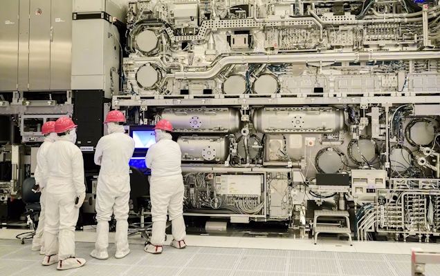
Intel’s High-NA EUV lithography system, built by ASML, during installation and calibration at Fab D1X in Hillsboro, Oregon, in April 2024.
Image credit: Intel Corporation