

Samsung Electronics and Broadcom have signed a memorandum of understanding (MoU) to expand their collaboration across advanced memory, semiconductor manufacturing and advanced packaging technologies. The initiative is aimed at supporting the next generation of artificial intelligence infrastructure, including AI accelerators, networking chips and high-performance computing (HPC) platforms.
According to Samsung, the cumulative value of the companies’ collaboration in memory and semiconductor manufacturing could exceed $200 billion over the next five years, through 2030. The company emphasized that this figure represents the projected scale of the planned partnership rather than a single purchase agreement or a binding financial commitment.
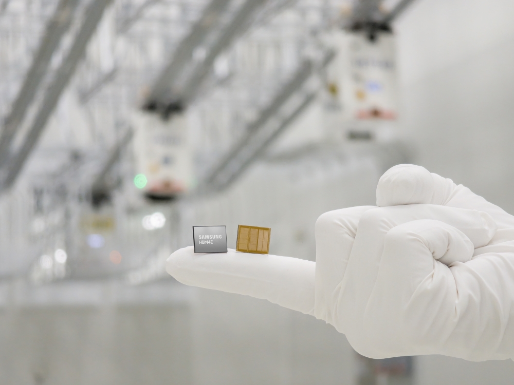
In the memory segment, the companies plan to expand their cooperation on advanced memory solutions, including High Bandwidth Memory (HBM), for future generations of Broadcom’s AI accelerators. HBM has become a critical component in AI systems and data centers by enabling high-speed data transfer between processors and memory.
Within the foundry business, the collaboration will focus on Samsung’s 2-nanometer and more advanced process technologies. These manufacturing nodes are expected to support Broadcom products for wireless communications, connectivity and AI infrastructure applications.
The companies also plan to integrate 2.3D and 2.5D advanced packaging technologies, enabling logic chips, memory and communication components to be combined within a single package. The approach is designed to increase bandwidth, improve overall system performance and reduce power consumption.
Young Hyun Jun, Vice Chairman and Head of Samsung Electronics’ Device Solutions Division, said that the rapid growth of AI is driving the need for tighter integration between memory, logic and advanced packaging. He added that the expanded collaboration with Broadcom will help deliver more integrated solutions for future AI infrastructure.
Charlie Kawwas, President of Broadcom’s Semiconductor Solutions Group, said that as AI infrastructure continues to scale, collaboration across the semiconductor ecosystem is becoming increasingly important to accelerate innovation.
The agreement could further strengthen Samsung’s position as an integrated supplier for the AI industry. The company is investing simultaneously in memory, foundry and advanced packaging technologies as it seeks to narrow the gap with TSMC in advanced semiconductor manufacturing and with SK hynix in the HBM memory market.
Credit: Samsung Electronics.