

Artificial intelligence, advanced manufacturing, high-bandwidth memory and new packaging technologies are reshaping the semiconductor industry. Based on the TechInsights Semiconductor Outlook 2026, this article explores five trends that are redefining how chips are designed, manufactured and deployed.
For decades, progress in the semiconductor industry was measured by one defining metric: transistor scaling. Each new process node delivered higher performance, greater transistor density and improved energy efficiency, extending the trajectory described by Moore’s Law.
That model continues to evolve, but it no longer explains the industry’s direction on its own.
Artificial intelligence has fundamentally changed the economics of semiconductor development. At the same time, chiplet architectures, high-bandwidth memory, advanced packaging and shifting geopolitical priorities are reshaping how next-generation computing platforms are built. Innovation is increasingly taking place at the system level, where manufacturing technology, processor architecture, memory, packaging and software evolve together rather than as separate disciplines.
The numbers illustrate the scale of this transformation. Following a record 2025, when the global semiconductor market reached approximately $796 billion, industry forecasts continue to point toward strong growth driven primarily by AI infrastructure, hyperscale data centres, advanced memory and packaging technologies. Under its most optimistic scenario, the TechInsights Semiconductor Outlook 2026 suggests the market could exceed $2 trillion before the end of the decade, reflecting the unprecedented level of investment now flowing into semiconductor technologies.
Against this backdrop, the TechInsights report identifies five developments that are expected to define the industry’s next phase of growth. Together, they reveal a broader shift in semiconductor innovation, one where competitive advantage depends not on a single technological breakthrough, but on the successful integration of multiple technologies across the entire computing ecosystem.
1. AI Is Rewriting the Economics of Chip Development
For more than a decade, smartphones were the semiconductor industry’s primary growth engine. Today, that role belongs to artificial intelligence.
The rapid expansion of generative AI, foundation models and high-performance computing has created unprecedented demand for advanced semiconductor devices. The effects extend far beyond AI accelerators themselves, influencing nearly every layer of the semiconductor value chain.
Industry projections indicate that the four largest US cloud providers are expected to invest approximately $718 billion in computing infrastructure and data centres during 2026. Those investments include far more than AI processors. They encompass high-bandwidth memory, ultra-fast networking, advanced packaging technologies and the infrastructure required to deploy increasingly sophisticated AI systems at scale.
The nature of processor development is changing as well.
While general-purpose CPUs remain indispensable, the strongest growth is occurring in specialised hardware designed specifically for machine learning workloads, including GPUs and application-specific integrated circuits (ASICs). At the same time, demand continues to rise for high-speed interconnects, advanced storage technologies and high-bandwidth memory, all of which are essential for feeding AI systems with the enormous volumes of data they require.
Another significant shift is taking place inside the world’s largest cloud companies. Rather than relying exclusively on merchant silicon vendors, hyperscalers are increasingly designing their own processors. Google’s Tensor Processing Units (TPUs), Amazon Web Services’ Trainium family and Microsoft’s Maia accelerators illustrate how semiconductor design has become a strategic capability for cloud infrastructure providers rather than remaining the exclusive domain of traditional chip manufacturers.
The result is a profound change in industry priorities. Artificial intelligence is no longer simply another application for semiconductors. It has become the primary force directing investment across processor architectures, manufacturing technologies, memory development, packaging strategies and networking infrastructure.
Meeting AI’s rapidly growing computational demands, however, requires more than larger data centres and increasingly powerful accelerators. It also depends on continued advances in semiconductor manufacturing, where each new process generation must deliver higher performance while operating within increasingly demanding power and thermal constraints.
2. Why 2 nm Is More Than Another Process Node
This is precisely where the transition to 2 nm becomes significant.
For decades, each new manufacturing node was largely associated with smaller transistors and higher transistor density. The move to 2 nm represents a much broader technological transition.
Further progress now depends on combining several major innovations, including Gate-All-Around (GAA) nanosheet transistors, backside power delivery, advanced materials and increasingly sophisticated manufacturing techniques. Together, these technologies enable further improvements in performance and energy efficiency even as conventional transistor scaling becomes progressively more difficult and expensive.
The first generation of 2 nm manufacturing is expected to deliver substantial gains in performance while reducing power consumption, particularly for AI accelerators, high-performance processors and hyperscale data centre applications. Achieving these improvements, however, comes at an extraordinary cost. Developing leading-edge manufacturing technologies now requires investments measured in tens of billions of dollars for a single fabrication facility, limiting participation to only a handful of companies worldwide.
TSMC is widely expected to lead volume production of 2 nm devices for customers including Apple and NVIDIA, while Samsung and Intel continue accelerating their own advanced manufacturing roadmaps as competition intensifies across the global foundry market. The race is no longer focused solely on technological leadership. Equally important is the ability to attract the next generation of AI, cloud computing and high-performance computing customers.
Not every application, however, requires the industry’s most advanced manufacturing node.
Industrial automation, automotive electronics, communications infrastructure and many embedded systems will continue to rely on mature process technologies for years to come. These applications often place greater value on reliability, manufacturing stability, long product lifecycles and cost efficiency than on maximum transistor density.
As a result, the semiconductor industry is evolving into a far more diverse manufacturing landscape. Leading-edge nodes will power the most demanding AI workloads, while mature technologies will remain essential across industrial, automotive and communications markets.
Competitive leadership is therefore being redefined. Process technology remains a critical differentiator, but it is no longer sufficient on its own. Success increasingly depends on the ability to combine advanced manufacturing with efficient chip design, sophisticated packaging technologies, advanced memory integration and a complete development ecosystem capable of supporting the next generation of computing platforms.
3. HBM4 Turns Memory into a Competitive Advantage
For years, processors dominated discussions about semiconductor innovation. In the AI era, memory has become equally critical.
As AI models continue to grow in size and complexity, moving data efficiently has become almost as important as processing it. Memory bandwidth is now one of the defining factors in overall system performance, making high-bandwidth memory one of the industry’s most strategic technologies.
HBM (High Bandwidth Memory) was developed specifically to address this challenge. By vertically stacking multiple DRAM dies using Through-Silicon Via (TSV) technology and placing memory close to the processor, HBM delivers dramatically higher bandwidth while reducing latency and improving energy efficiency compared with conventional DRAM architectures.
The industry is now preparing for the next step.
HBM4 is expected to deliver higher capacity, increased bandwidth and improved scalability for the next generation of AI accelerators and high-performance computing platforms. The transition, however, involves far more than introducing a faster memory device.
One of the most significant architectural changes is the growing adoption of sophisticated logic base dies, manufactured using advanced foundry processes rather than conventional DRAM fabrication alone. This logic layer provides higher I/O performance, improved memory management and greater flexibility for future AI systems. It also creates a direct link between advanced logic manufacturing, memory innovation and next-generation packaging technologies.
As AI deployments continue to accelerate, HBM has become one of the fastest-growing segments of the memory market. SK hynix, Samsung and Micron are investing billions of dollars to expand production capacity while developing future HBM generations. For processor manufacturers, memory availability has become a strategic consideration that directly influences the delivery of AI accelerators to market.
The industry’s approach to memory is changing accordingly.
Memory is no longer a supporting component that follows processor development. It is becoming an integral part of system architecture, designed alongside processors, manufacturing technologies and advanced packaging. As AI systems continue to scale, overall performance will increasingly depend on how effectively these elements operate as a single platform.
That growing level of integration naturally leads to the next transformation: the package itself is becoming as important as the silicon it contains.
4. Advanced Packaging Moves to the Centre of Semiconductor Innovation
For decades, packaging was viewed as the final stage of semiconductor manufacturing. Today, it is one of the industry’s primary innovation drivers.
As transistor scaling becomes more challenging and economically demanding, semiconductor companies are finding new ways to improve performance by redesigning how chips are integrated rather than relying solely on smaller process nodes.
The most visible example is the widespread adoption of chiplet architectures.
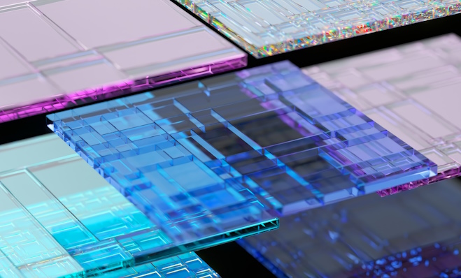
Instead of integrating every function onto a single monolithic die, designers increasingly divide complex processors into multiple specialised chiplets that are combined within a single package. This modular approach allows each function to be manufactured using the process technology best suited to its requirements, improving yields, reducing development costs and accelerating product development.
Making this approach practical depends on equally sophisticated packaging technologies.
Silicon interposers, hybrid bonding and advanced three-dimensional integration techniques enable extremely high-bandwidth communication between chiplets while reducing latency and power consumption. The package is no longer simply protecting the silicon. It has become an active part of the computing architecture itself.
The AI boom has highlighted just how strategically important packaging has become.
Demand for AI accelerators has, at times, been constrained not by wafer fabrication capacity but by the availability of advanced packaging technologies such as TSMC’s CoWoS platform. This has prompted foundries and semiconductor manufacturers to invest heavily in expanding advanced packaging capacity, recognising that future competitiveness depends as much on packaging as on wafer production.
The shift extends well beyond manufacturing.
Modern AI systems increasingly combine CPUs, GPUs, HBM stacks, networking interfaces and custom accelerators within a single package. Designing these heterogeneous systems requires close collaboration across processor architecture, memory, packaging and thermal engineering. System performance is increasingly determined by how effectively these technologies work together rather than by the capabilities of any individual device.
Advanced packaging has therefore evolved from a manufacturing step into a core engineering discipline. As computing platforms become more complex, it will play an increasingly central role in determining performance, scalability and energy efficiency.
The growing complexity of these integrated systems also raises another challenge. Building the world’s most advanced computing platforms now depends on a highly interconnected global supply chain.
5. Geopolitics Becomes a Strategic Design Constraint
For decades, the semiconductor industry was built around a highly specialised global supply chain.
Chip design was concentrated largely in the United States, advanced manufacturing in Taiwan and South Korea, while assembly, packaging and testing were distributed across Southeast Asia. This global model maximised efficiency by allowing each region to specialise in different parts of the value chain.
That model is now evolving.
The Covid-19 pandemic, geopolitical tensions and the strategic importance of advanced semiconductors exposed the vulnerability of highly concentrated supply chains. National security, technological sovereignty and supply chain resilience have become central considerations alongside traditional business and engineering priorities.
Governments have responded with ambitious industrial strategies.
The United States, the European Union, Japan and several other countries are investing heavily in domestic semiconductor manufacturing through subsidy programmes, tax incentives and long-term industrial policies. At the same time, semiconductor companies are expanding production across multiple regions in an effort to reduce dependence on individual manufacturing locations.
Complete technological independence, however, is neither practical nor desirable.
Advanced semiconductor development depends on an ecosystem that spans electronic design automation software, manufacturing equipment, materials, intellectual property, wafer fabrication and advanced packaging. These capabilities remain distributed across multiple regions, making international collaboration essential to continued innovation.
The industry’s challenge is therefore shifting from maximising efficiency to balancing efficiency with resilience.
Future semiconductor leadership will depend not only on technological excellence, but also on the ability to build secure, diversified and flexible supply chains capable of supporting increasingly complex AI-driven computing platforms.
Conclusion
The five trends identified in the TechInsights Semiconductor Outlook 2026 describe more than the next stage of semiconductor development. Together, they illustrate a fundamental shift in how innovation is created across the industry.
Progress is no longer defined solely by transistor scaling or a single breakthrough in manufacturing technology. Competitive advantage increasingly emerges from the integration of advanced process technologies, heterogeneous architectures, high-bandwidth memory, sophisticated packaging and resilient global supply chains.
Artificial intelligence sits at the centre of this transformation.
Its growing computational demands are reshaping processor design, accelerating the transition to advanced manufacturing nodes, driving demand for next-generation memory and making advanced packaging a strategic technology in its own right. At the same time, geopolitical priorities are influencing where these technologies are developed, manufactured and deployed.
Viewed together, these trends point to a new model of semiconductor innovation. Future leadership will depend less on excellence in any single discipline and more on the ability to combine manufacturing, architecture, memory, packaging and software into highly integrated computing platforms.
The next era of semiconductors will not be defined by one technology alone. It will be shaped by how successfully the entire ecosystem evolves as a unified engineering system.
This article is based primarily on the TechInsights Semiconductor Outlook 2026 report, complemented by additional industry data and publicly available information.
By New-Tech Magazine Group Team


