



The next era of semiconductor and PCB design will be defined by two parallel imperatives: making core engines faster and making engineers more productive. On the engine side, the industry is embedding machine learning and reinforcement learning directly into EDA tools – enabling, for example, local models built from a small set of SPICE simulations to dramatically accelerate verification while maintaining near-SPICE accuracy. Simultaneously, leading EDA vendors are partnering with hardware companies such as NVIDIA to GPU-accelerate core algorithms, unlocking vastly higher throughput across simulation, design exploration, coverage analysis, and OPC. Addressing the second imperative of engineering productivity demands a fundamentally different kind of AI solution.
For faster engineers, generative EDA AI copilots were the industry’s first answer – but they are no longer sufficient. As design complexity and tool fragmentation accelerate, manual scripts and isolated point solutions fail to scale. Engineers need more than a chatbot; they need autonomous systems capable of intelligent reasoning, multi-step execution, and real-time adaptation across diverse EDA tools. This is the promise of agentic automation: a unified orchestration layer that delivers expert-level decision-making across the complete design lifecycle. Realizing it, however, requires overcoming domain-specific hurdles that generic AI frameworks are simply not equipped to handle.
Five Core Challenges of EDA Complexity
Generic, off-the-shelf AI models struggle with chip design because the industry relies on a highly specialized foundation. Any solution must seamlessly span the entire end-to-end workflow – from initial concept to manufacturing sign-off – automating critical tasks across front-end design, verification, physical implementation, PCB sign-off, and manufacturing readiness to serve as a true unified intelligence layer.
To effectively deploy agentic AI in EDA, developers must address five distinct challenges:
- Proprietary Chip Design Expertise: Chip design relies on physics-based methodologies absent from public training data. Generic agents lack the specific expertise needed to configure specialized tools, orchestrate sequences, or generate precise production code.
- Rigid EDA Environments and Data Flows: EDA relies on secure, on-premise clusters rather than fast cloud frameworks. Agents must manage long-running verification jobs, integrate with legacy schedulers (such as LSF), and handle terabyte-scale datasets in-place.
- Scalability Across Fragmented Workflows: The vast EDA tool ecosystem can easily overwhelm standard AI, leading to “context saturation” and hallucinations. A unified orchestration layer is essential for deterministic execution across expanding tool chains. Critically, because EDA workflows are inherently multi-vendor and cannot be confined to a specific ecosystem, AI agents require high flexibility to operate seamlessly across diverse toolsets.
- Opaque EDA Modalities: EDA data involves dense binary formats and opaque databases. Agents require domain-specific parsers to extract actionable intelligence from complex artifacts like waveforms and netlists.
- Embedded Enterprise Security: To safeguard sensitive IP, agents must operate in highly secure environments. This requires robust Role-Based Access Controls (RBAC), strict sandboxing, comprehensive audit trails, and human-in-the-loop checkpoints.
The Solution: Siemens’ Fuse EDA AI System and Fuse EDA AI Agent
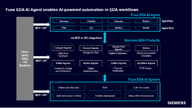
To address these highly specific industry bottlenecks, Siemens has introduced the Fuse™ EDA AI System and Fuse™ EDA AI Agent. This system fundamentally transforms chip and PCB design by integrating generative and agentic AI capabilities across the complete Siemens EDA portfolio. Through a context-aware natural language interface, it intelligently orchestrates complex, multi-tool workflows from initial concept through manufacturing sign-off, increasing engineering productivity and design quality.
The architecture is purpose-built for semiconductor engineering. At its core is a centralized, multimodal EDA data lake that uses specialized parsers to break down team and tool silos, ensuring every workflow operates from a single source of truth. Layered on top is an advanced RAG framework trained on Siemens EDA tools and methodologies, enabling the system to answer complex domain-specific queries with precision rather than approximation. The system is also model-agnostic and open by design – supporting multiple LLMs and integrating seamlessly with third-party tools, reflecting the reality that production EDA environments are inherently multi-vendor. Security and deployment flexibility are built in from the ground up, with support for both on-premises and cloud environments, native RBAC, and comprehensive audit trails that safeguard IP at every layer.
(Source: Siemens Digital Industries Software)
Bringing these capabilities together is the Fuse EDA AI Agent, delivering end-to-end automation by planning, orchestrating, and executing workflows across the full semiconductor and PCB system design cycle. This is complemented by AI-driven tool automation and natural-language debugging, allowing engineers to express intent in plain language and have the system translate it into precise, executable actions. Fuse EDA AI Agent also solves scalability issues by centralizing tool discovery within a unified operational layer, effectively preventing context saturation as workflows expand. Ultimately, this creates a system that goes beyond basic assistance, operating autonomously and reliably on behalf of engineers at an enterprise scale.
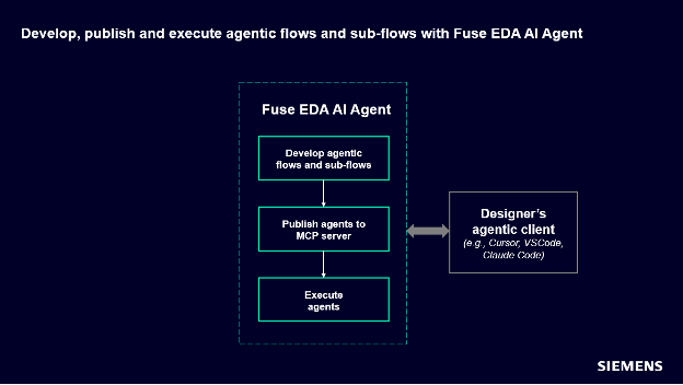
The Fuse EDA AI Agent is built on a highly modular philosophy: each sub-flow from the broader EDA workflow is automated in detail. This is accomplished using a combination of the Model Context Protocol (MCP) for executing EDA tools, “Agent Skills”—executable playbooks that encode domain expertise to properly sequence and set up tools with built-in validation and guardrails—and specialized EDA parsers within Fuse EDA AI System to extract precise context from complex EDA data formats (e.g., LEF/DEF, GDSII). Once hundreds of these automated sub-flows are developed, they can be strung together to construct comprehensive, multi-tool workflows that span the entire EDA lifecycle. It is much like taking individual Lego pieces to build increasingly larger, modular structures.
(Source: Siemens Digital Industries Software)
The Future: A New Era of EDA Automation
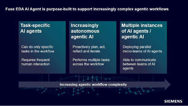
The introduction of solutions like the Fuse EDA AI Agent marks the beginning of a fundamental shift in how semiconductor and PCB design are conducted. Today’s AI agents are already handling narrow, repetitive workflows, boosting productivity while engineers remain in control of higher-level decisions. But this is only the starting point.
As AI agents grow more capable, they will evolve from reactive task executors into proactive design assistants – autonomously managing entire EDA phases, reasoning through complex trade-offs, and self-correcting without manual intervention. Looking further ahead, collective intelligence at scale will redefine what is possible: the engineer’s role will shift from task execution to strategic supervision, overseeing hundreds of parallel agents simultaneously optimizing across power, performance, and area at a scale no human team could match alone.
(Source: Siemens Digital Industries Software)
Semiconductor and PCB design stand at an inflection point. The shift from copilots to autonomous agents is not a distant prospect – it is already underway. Over the next few years, multi-agent AI systems will fundamentally reshape the design lifecycle, compressing timelines, democratizing expertise, and unlocking levels of parallel innovation that were previously impossible. The architectures being built today are laying the critical groundwork for this autonomous EDA future. Explore Fuse™ EDA AI Agent to start your AI-powered EDA journey.
Author: Niranjan Sitapure, Central AI Product Manager, Siemens EDA
Niranjan Sitapure, PhD, is the Central AI Product Manager at Siemens EDA. He oversees road mapping, development, strategic AI initiatives, and product marketing for the Siemens EDA AI portfolio. With a PhD in Engineering from Texas A&M University, Niranjan has deep expertise in advanced AI and machine learning technologies, including time‑series transformers, large language models (LLMs), and digital twins for engineering applications. Previously, Niranjan was a consultant at Bain & Company, where he advised Fortune 500 and Private Equity clients on digitization strategies, operating model redesigns, and due diligence.