
Automotive application circuits must meet strict EMI standards to avoid interfering with broadcast and mobile service frequency bands. In many cases, Silent Switcher® and Silent Switcher 2 solutions can make a significant difference in the ability to meet these standards. Nevertheless, in all cases, careful layout is imperative. In this article we look specifically at two possible solutions for a 4-switch buck-boost controller and compare EMI chamber results.
A 4-switch buck-boost combines a buck and boost controller into a single IC, where the converter operates as a buck when the output is lower than the input, and as a boost when the output is higher than the input. In the region where the output and input are similar, all four switches may operate.
Using ADI’s in-house EMI chamber at Santa Clara, CA, the Power Products research team launched an investigation into the effectiveness of the original dual hot loop synchronous layout and if an alternative layout could be used for lower EMI noise to pass the EMI standard.
The dual hot loop layout involves the symmetrical placement of hot loop ceramic capacitors around power MOSFETs to contain EMI noise. ADI’s unique sense resistor location—alongside the inductor and outside of the hot loops—allows these loops to be very small, and thus minimize the antenna effect of the hot loops. To achieve this symmetry and enable the switch node(s) to reach the nearby inductor, switching node vias are required, which may compromise the hot loop area. Using the CISPR 25 compliant EMI chamber, the research team found that exposure of the switching node and large hot loop area results in unwanted conducted EMI especially at >30 MHz (the FM radio band), which is the most challenging frequency range to attenuate.
The original buck-boost layout, which has a single hot loop, can improve its smallest hot loop by rearranging the power MOSFETs and hot loop capacitors. This layout is known as a single hot loop as a counterpart of the dual hot loop. The benefit of using a single hot loop is not only smaller switching loss but also that >30 MHz conducted emissions (CE) are attenuated due to the minimized hot loop area and the exposure of the switching node. Its effectiveness is verified by comparing the EMI noise of the new layout to a dual hot loop using the same controller IC and same power components. A 4-switch buck-boost controller, LT8392, and its two versions of demo circuit (DC2626A rev.2 and rev.3) were used for the experiment.
Layout Comparison
Figure 1 shows the layout and assembled board pictures of a dual hot loop and single hot loop. Each board has four layers: a top layer (Layer 1), Layer 2, Layer 3, and a bottom layer (Layer 4). However, only the top and bottom layers are shown. As shown in Figure 1(a), hot loop capacitors are placed at the left and right side of the center MOSFETs and form identical hot loops. Switching node vias are used to connect the switching nodes, SW1 and SW2, to the main power inductor through the bottom layer (shown in Figure 1(c)) and Layer 3. The SW1 and SW2 top layer copper nodes are laid out with large area to dissipate the heat of the inductor and MOSFETs. But at the same time, the largely exposed SW1 and SW2 copper nodes are a source of EMI emission. If the board is mounted near chassis ground, parasitic capacitance is formed between the chassis and the switching node copper. It makes high frequency noise flow from the switching node to chassis ground and affects other circuits in the system. In the CISPR 25 compliant EMI chamber, the high frequency noise flows through the ground table of the EMI setup and LISN. The exposed switching node also acts as an antenna and, thus, causes radiated EMI noise.
However, a single hot loop does not have the exposed switching node copper at the bottom layer, as shown in Figure 1(d). At the top layer, shown in Figure 1(b), the hot loop capacitors are placed at only one side of the MOSFETs, which makes it possible for the switching node to be connected to the inductor without using switching node vias.
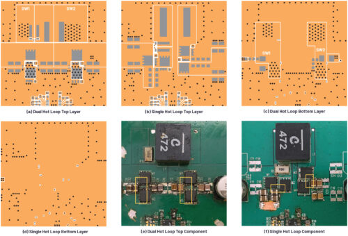
Figure 1. Layout and photograph of a dual hot loop and single hot loop.
In the single hot loop layout, the top and bottom MOSFETs are not aligned, but one of them is 90° rotated to make the hot loop as small as possible. The size of the hot loop of the dual hot loop and the single hot loop are compared in Figure 1(e) and Figure 1(f) with the yellow highlighted box. These boxes show that the hot loop of a single hot loop is half the size of the dual hot loop.
It should be noted that the two 0402 hot loop capacitors of the dual hot loop shown in Figure 1(a) are not used and the 1210 hot loop capacitors are squeezed to the MOSFETs to make the smallest hot loop.
A solder mask near the 0402 capacitor pads is peeled off for good connectivity of 1210 capacitors. Also, the solder mask near the inductor pad is removed to use the same inductor in the single hot loop circuit. A smaller hot loop means that the total inductance of the loop is smaller. Thus, switching loss is reduced and LC ringing of the switching node and switching current is attenuated. Also, the smaller loop contributes to lower conducted EMI above 30 MHz as radiated emissions affect conducted EMI in that range.
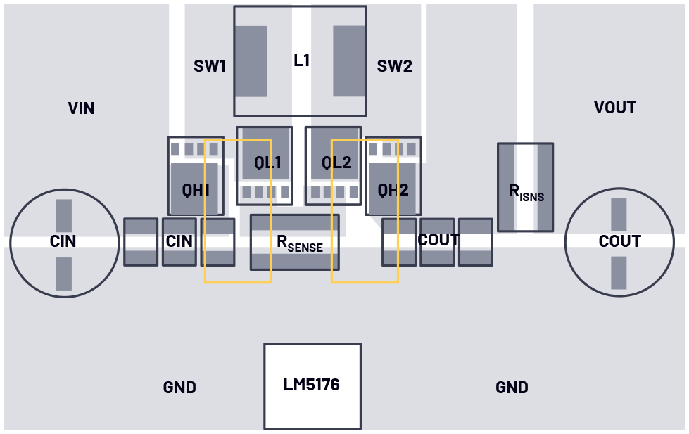
Figure 2. The recommended buck-boost layout of competitor part LM5176.
ADI’s 4-switch buck-boost controller can form the smallest hot loop due to the proprietary peak buck/peak boost current-mode control scheme. The current sense resistor is connected in series with the main inductor. In contrast, competitors’ controller parts use a valley buck/peak boost current-mode control scheme where the current sense resistor should be put between the source of the bottom MOSFETs and ground. Figure 2 shows the recommended buck-boost layout of one of these parts. As shown with the yellow box, the hot loop is larger than the dual hot loop or single hot loop. Moreover, the parasitic inductance of the sense resistor increases the total inductance of the hot loop.
EMI Comparison
The EMI of the dual hot loop and single hot loop is measured in the CISPR 25 compliant EMI chamber and shown in Figure 3 with a CISPR 25 Class 5 standards limit. The EMI results are plotted in the same graph to compare the difference, with a dual hot loop marked with a yellow line and a single hot loop marked with a red line. The gray line is the noise floor that is measured at ambient condition. As shown in Figure 4, the exposed switching nodes of the bottom layers of a dual hot loop were ground shielded with copper tape to show how effective the smaller hot loop is. The emission of a dual hot loop without the copper shield is much higher than the result in Figure 3. The output is 12 V, 8 A and the input voltage was set to 13 V to make the circuit operate in 4-switch switching mode.
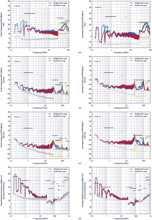
Figure 3. EMI comparison graph of a dual hot loop and single hot loop: (a) voltage method conducted emissions peak and average, (b) current probe method conducted emissions 50 mm peak and average, (c) current probe method conducted emissions 750 mm peak and average, and (d) radiated emissions vertical peak and average.
Figure 3(a) shows the peak and average of voltage method conducted emissions, respectively. A single hot loop has 5 dBµV lower CE above 30 MHz and it satisfies the CISPR 25 Class 5 standard for both peak and average CE while dual hot loops have overshoot in average at FM and VHF band (68 MHz to ~108 MHz), as shown in the yellow highlighted box.
Note that reducing 5 dBµV in that frequency range is really challenging. A single hot loop is effective not only at the high frequency range of 30 MHz, which is the most challenging region to attenuate, but also at low frequency (<2 MHz) that includes AM band (0.53 MHz to ~1.8 MHz). It is always better to have lower emissions, especially if they are CE, since they affect all of an electrically connected system.
The current probe method is another measurement method that CISPR 25 Class 5 specifies. It measures common-mode conducted emissions at two different positions, 50 mm and 750 mm from DUT, while the voltage method measures mixed conducted emissions of both common mode and differential mode. Figure 3(b) and 3(c) compare the current probe method conducted emissions of the dual hot loop and single hot loop. They show that the single hot loop has lower conducted emissions above 30 MHz, and especially at FM band, as shown in the yellow highlighted boxes. Unlike the voltage method conducted emissions, there is no significant benefit of a single hot loop over dual hot loop at the low frequency around the AM band.
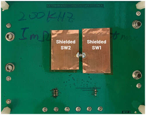
Figure 4. Shielded switching nodes of bottom layer of a dual hot loop.
Lastly, Figure 3(d) shows the radiated emissions (RE) of the two different buck-boost layouts. The results are almost identical except that the dual hot loop has a spike around 90 MHz, which is 5 dBµV/m higher than the single hot loop.
Thermal Comparison
A thermal comparison between the dual hot loop and the single hot loop is made in Figure 5. The thermal images are taken at 9.4 V input voltage with SSFM on. 9.4 V is the lowest point of the 4-switch operation region before the operating mode is changed to 2-switch pure boost when the output voltage is 12 V. Thus, the test condition is the harshest. The hottest component of the dual hot loop, the boost-side bottom MOSFET, and the single hot loop have almost the same temperature. Although the single hot loop does not have the switching node vias and copper at the bottom layer that can dissipate heat, its switching loss is lower than the dual hot loop due to the smaller hot loop. Also, by not using the switching node vias, the single hot loop has better heat dissipation at the top layer because the contact area of the MOSFET drain pad and the switching node copper is larger than that of the dual hot loop.
Conclusion
The suggested new buck-boost layout, single hot loop, is recommended for new, high power designs. Due to the minimized exposure of the switching node and the hot loop area, the single hot loop has significant benefit to reduce both conducted and radiated emissions without any thermal disadvantages. Notably, it reduces conducted emissions above 30 MHz, which is the most challenging frequency region to attenuate. Thanks to the proprietary peak buck/peak boost current-mode control feature of ADI’s 4-switch buck-boost controllers (LT8390/ LT8390A, LT8391/LT8391A, LT8392, LT8393, LT8253, etc.), the hot loop can be made much smaller than those with competitors’ parts. The control feature results in higher efficiency and lower EMI, making ADI’s 4-switch buck-boost controllers the best choice for automotive applications or any EMI sensitive applications.
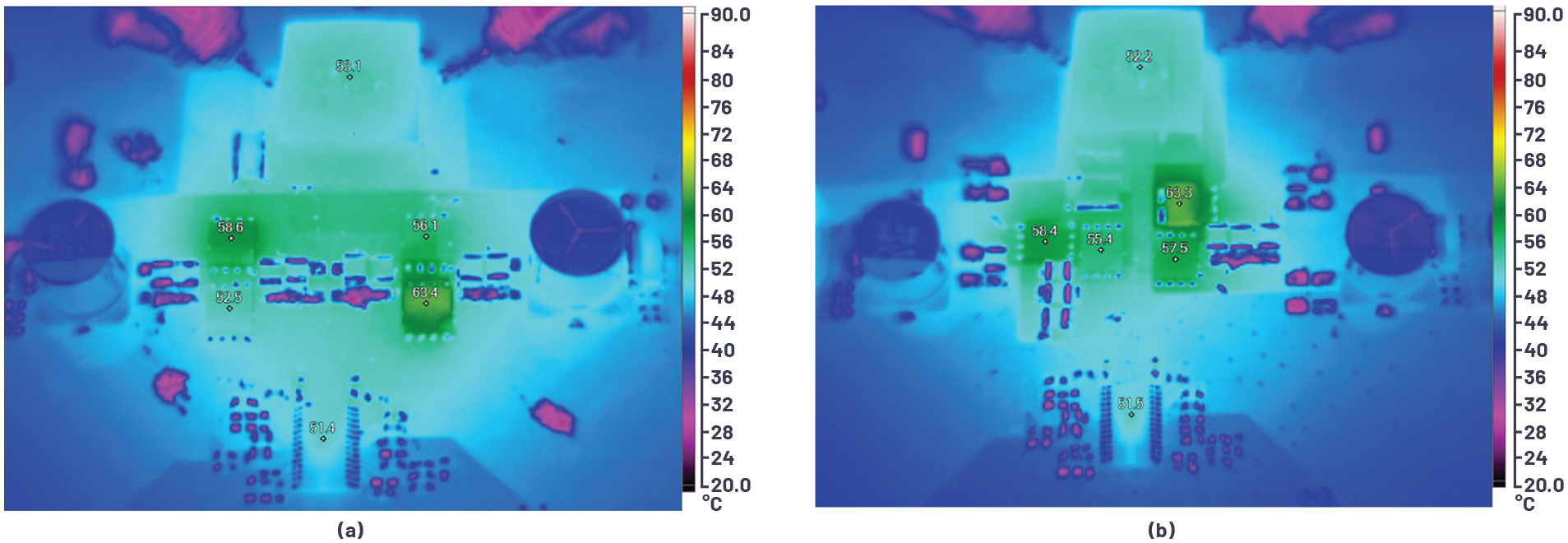
Figure 5. (a) Thermal image of a dual hot loop, and (b) thermal image of a single hot loop.