
Samsung ‘X-Cube’ enables industry-first 3D SRAM-logic working silicon at 7nm and beyond.
Bandwidth and density can be scaled to suit diverse design requirements in emerging applications.
Samsung Electronics, a world leader in advanced semiconductor technology, today announced the immediate availability of its silicon-proven 3D IC packaging technology, eXtended-Cube (X-Cube), for today’s most advanced process nodes. Leveraging Samsung’s through-silicon via (TSV) technology, X-Cube enables significant leaps in speed and power efficiency to help address the rigorous performance demands of next-generation applications including 5G, artificial intelligence, high-performance computing, as well as mobile and wearable.
“Samsung’s new 3D integration technology ensures reliable TSV interconnections even at the cutting-edge EUV process nodes,” said Moonsoo Kang, senior vice president of Foundry Market Strategy at Samsung Electronics. “We are committed to bringing more 3D IC innovation that can push the boundaries of semiconductors.”

*The image shown is for illustration purpose only.
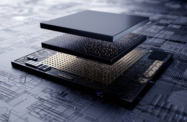
With Samsung’s X-Cube, chip designers can enjoy greater flexibility to build custom solutions that best suit their unique requirements. The X-Cube test chip built on 7nm uses TSV technology to stack SRAM on top of a logic die, freeing up space to pack more memory into a smaller footprint. Enabled by 3D integration, the ultra-thin package design features significantly shorter signal paths between the dies for maximized data transfer speed and energy efficiency. Customers can also scale the memory bandwidth and density to their desired specifications.
Samsung X-Cube’s silicon-proven design methodology and flow are available now for advanced nodes including 7nm and 5nm. Building on the initial design, Samsung plans to continue collaborating with global fabless customers to facilitate the deployment of 3D IC solutions in next-generation high-performance applications.
More details on Samsung X-Cube will be presented at Hot Chips, an annual conference on high-performance computing, which will be livestreamed Aug. 16-18.
