

Automated, integrated validation earlier in the design flow accelerates cycle-time, increases reliability, and reduces risk and costs.
With the increasing complexities of advanced systems design, and competitive threats in delivering innovative products to market faster, engineering management needs to seek and adopt new technologies to succeed in today’s global economy. The traditional project development flow is inefficient and fraught with pitfalls. It relies far too heavily on manual reviews and costly prototypes. Verification of each design phase occurs far too late in the process.
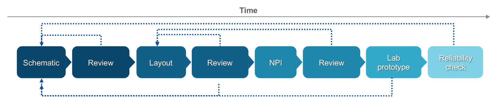
Figure 1 – The conventional project development flow
The key to a more efficient design flow is the early detection and elimination of potential design issues. These potential issues include simple schematic errors that are allowed to propagate forward into layout, complex mechanical issues, and factors that impact product testability and manufacturability.
Identifying and fixing these potential problems as early in the process as possible—a “shift left” of these activities—avoids unnecessary schedule delays and costly design respins. It also frees up valuable engineering talent to move on to other projects.
A shift-left methodology relies upon a fully-inclusive system design platform for upfront design analysis and verification. This solution integrates a broad range of analysis and verification tools during the schematic and layout phases of the project. These tools are aimed at non-specialist PCB design engineers and layout designers and allow them to work within their familiar authoring environments to identify problems early.
An integrated verification flow starts at the source – the schematic. Errors caught and fixed here have the greatest impact on the rest of the process. They are also, traditionally, the ones most likely to slip through the cracks and go undetected using conventional manual review processes. Relying on a “second set of eyes” to review a complex design with multiple PCBs and thousands of components is time consuming, limited in scope and error-prone. It adds time to the schedule, consumes valuable engineering talent and still allows many simple, easily fixed schematic errors to be passed through to layout and subsequently hard-wired into physical prototypes.
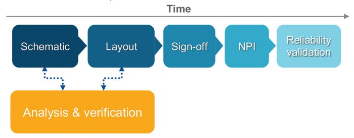
Figure 2 – A shift-left approach for integrating verification into the design process.
Automated schematic integrity analysis replaces the manual review process. It enables full inspection of all nets in the design, for both single and multi-board designs, using pre-defined checks for common schematic errors and an intelligent component model library. This analysis is performed in parallel with schematic entry and eliminates most common schematic errors before layout starts. The design checks are power and technology aware. Replacing the manual review process with an automated one results in greater coverage and much higher probability of entering layout with a schematic that will provide first-pass success.
Testability analysis should also occur during schematic entry, prior to layout. The goal is to move testability analysis to earlier in the design flow and automate the process. The design is analyzed, test point requirements are identified and passed to layout as constraints. The result is fewer errors due to insufficient test coverage, a quicker and smoother handoff to manufacturing with more efficient and cost effective test processes.
Signal integrity, power integrity and analog/mixed signal simulations and analysis should also take place during the schematic phase of the design. This allows the designer to develop a set of placement, routing and PDN constraints that meet the target design requirements. As with the test point requirements, these constraints are passed forward to layout.
During layout, signal integrity analysis is performed on all critical nets to ensure both signal quality and timing requirements are within spec. Power integrity analysis should include both DC drop analysis to identify excessive voltage drops and high current densities, as well as AC power plane analysis to optimize capacitor selection and placement.
As component placement is progressing, EMI validation, thermal analysis, vibration/acceleration and manufacturability analysis should all be performed to quickly identify and correct any potential issues. In the traditional design flow, these issues would not be discovered until physical testing in an EMI, thermal or HALT test chamber. If they are not caught during layout, issues that impact the mechanical integrity of the design are usually the most expensive and time consuming to fix. Such issues often require board re-spins and tooling changes to correct. Simulations during layout greatly increased the likelihood of first-pass success.
A post layout sign-off phase should include both electrical rule checking and design-for-manufacturing validation. In the conventional design flow, validation of the electrical performance of a design is often done by visual inspection by manually scanning through multiple PCB layers for ground return paths, potential noise sources and other layout related problems. Again, this is a process that should be automated by running a full board verification against a set of pre-defined rules. Finally, design-for-manufacturability verification should be performed to ensure the cost effective manufacturability of the final product. This should be a comprehensive analysis covering the fabrication, assembly and test of standard PCBs, rigid-flex and multi-board designs.
The motivation of the shift-left approach is the same in all cases — to move as much verification as possible as early in the design cycle as permissible, while also automating the analysis to provide the highest possible degree of coverage. Identifying and correcting issues at the source eliminates time consuming debug efforts and costly respins. The conventional design flow is frustratingly unpredictable. It relies far too much on manual visual design checks that allow far too many errors to propagate forward to the next step in the process. The shift-left automated verification flow catches errors and identifies potential issues early in the process where they are quickly and economically corrected. It is a more efficient process that provides more predictable results, eliminates design re-spins and yields higher quality products in less time.
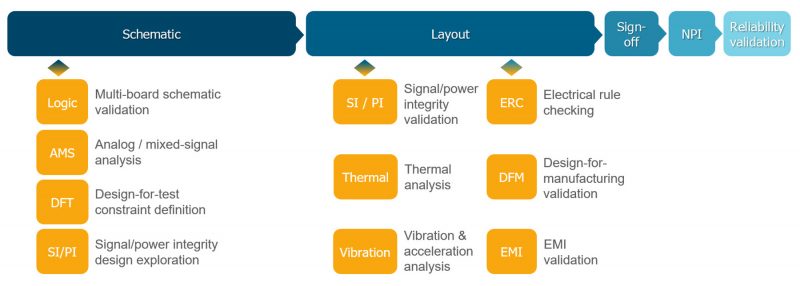
Figure 3 – An inclusive multi-dimensional verification process
The ultimate goal should be an all-inclusive, multi-dimensional verification process that reduces reliance on both manual reviews and manual debugging of physical prototypes. Mentor, A Siemens Business, is the first electronic design software company with a broad portfolio of proven technologies to enable shift-left design verification. Its fully-integrated Xpedition® verification platform for single and multi-board PCB system design includes automated schematic integrity analysis with built-in automated design checks and an extensive library of intelligent models. Testability analysis, automated component modeling for vibration analysis, DC voltage drop analysis for rigid-flex and multi-board designs, as well as concurrent DFM analysis during layout, are additional technologies integrated within the authoring environment for easier, faster validation.
The benefits of this new multi-dimensional verification platform are the reduction of costly design respins, improved time-to-market for new products, and the development of higher quality products with fewer defects.
David Wiens, Xpedition Product Manager, System Design Division, Mentor, A Siemens Business
Over the past 30+ years, David Wiens has held various engineering, marketing and management positions within the EDA industry. His focus areas have included advanced packaging, high-speed design, routing technology and integrated systems design. He is currently the product manager for the Xpedition Enterprise portfolio of products for electronics systems design. He holds a B.S. in computer science degree from the University of Kansas.
