

A phase-locked loop (PLL) circuit is a feedback system that combines a voltage controlled oscillator (VCO) and a phase detector in such a way that the oscillator signal tracks an applied frequency or phase modulated signal with the correct frequency and phase. PLLs are used when stable, higher output frequencies need to be generated from fixed low frequency signals or when rapid frequency changes are necessary. Typical use cases are in high frequency, telecommunications, and measurement technology for realizing filters, modulation, and demodulation, as well as for frequency synthesis.
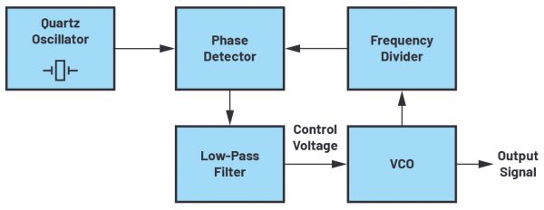
Figure 1: Block diagram of a phase-locked loop
Figure 1 shows a block diagram of a PLL-based frequency synthesizer. The VCO generates the output signal. It is maintained at the setpoint frequency by the PLL and locked to the reference frequency. The reference frequency is typically supplied by a very accurate quartz oscillator. A frequency divider is provided in the feedback path of the phase-locked loop circuit in front of the phase detector to reduce the VCO frequency by an adjustable factor.
A VCO contains an adjustable tuning element, such as a varactor diode with a capacitance that changes depending on the input voltage. The PLL circuit is thus a kind of feedback control system for the VCO. The required input or control voltage to the VCO is often higher than the supply voltage available to the PLL circuit. The supply voltage is typically 3.3 V or 5 V, whereas VCOs may require voltages of more than 20 V depending on the desired frequency. To generate a wider range of frequencies, VCOs with a wider tuning range can be used. A simplified circuit example that supports VCOs in the gigahertz range is shown in Figure 2.
As a VCO, the DCYS100200-12 from Synergy Microwave Corporation can be used. It allows a frequency of 2 GHz at 28 V (VTUNE), as can be seen in the graph in Figure 3.
There are several possibilities for generating the high control voltage. One is using an active loop filter, which essentially consists of a high speed amplifier and a low-pass filter that shapes the output pulses from the phase detector (CPOUT) into a clean dc voltage. As an alternative to this, a PLL frequency synthesizer with an integrated charge pump, such as the ADF4150HV from Analog Devices, Inc. (ADI), which does not require an additional active loop filter, can be used. Although both solutions require a high voltage supply, the number of components can be reduced with the ADF4150HV. The distortion and phase noise caused by the active filter amplifier can also be avoided. Furthermore, the ADF4150HV permits implementation of fractional-N or integer-N phase-locked loop frequency synthesizers. Thus, the VCO frequency can be divided by 1, 2, 4, 8, or 16 so that output frequencies down to a minimum of 31.25 MHz are possible.
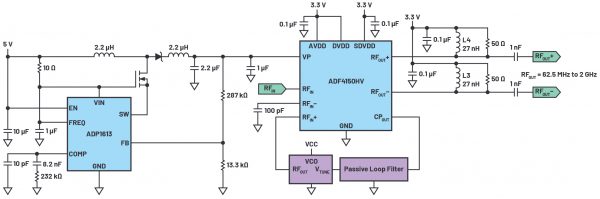
Figure 2: Simplified circuit of a high voltage charge pump supply for the ADF4150HV.
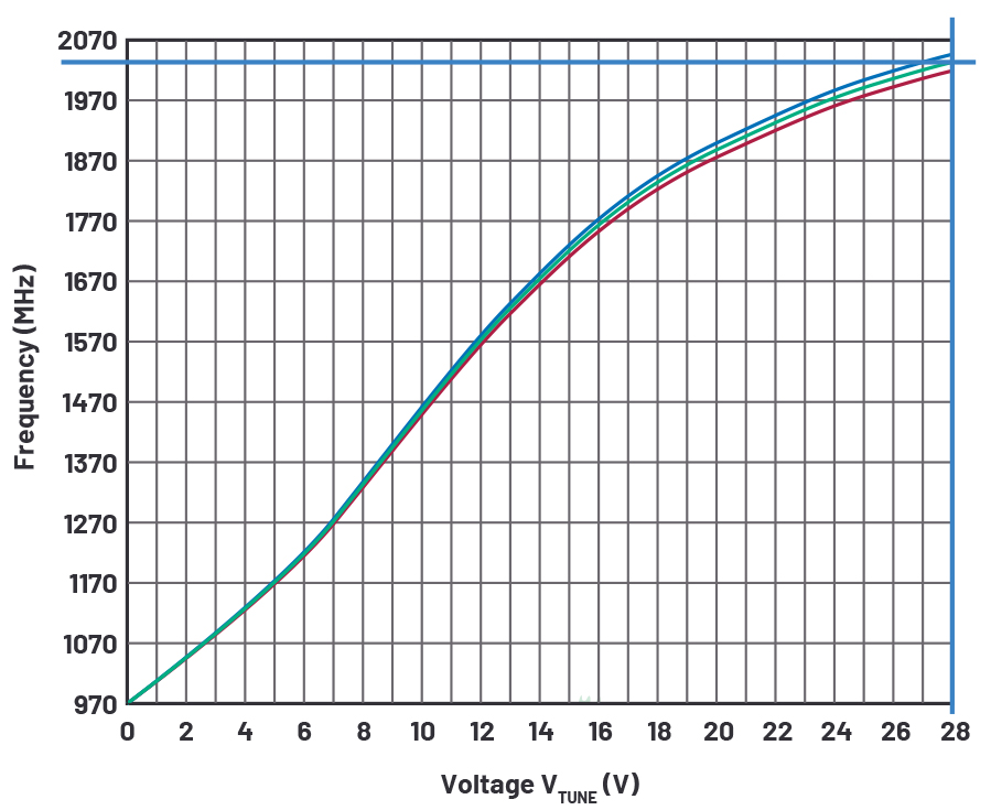
Figure 3: Control voltage vs. frequency of the DCYS100200-12.1
The high voltage required for the ADF4150HV’s integrated charge pump can be generated with the dc-to-dc boost converter ADP1613 without any compromises in PLL performance. The ADP1613 is an effective switching regulator with integrated power transistor for easily achieving output voltages of up to 20 V. Higher output voltages are also possible by using additional external components, especially through an external power transistor. The switching frequency of the ADP1613 can be adjusted in a range from 650 kHz to 1.3 MHz. This leads to a better transient response and simple noise filtering. In general, selecting a switching frequency of greater than 1 MHz is recommended so that switching noise can be reduced by the PLL loop filter.
The phase-locked loop frequency synthesizer circuit with the ADF4150HV offers an ultrawideband PLL function with use of the integrated RF divider. It enables a frequency coverage of 62.5 MHz to 2 GHz. With the same PLL hardware design, different frequencies can be generated for a multitude of different hardware platforms in the system. However, if a design is required for various VCO types, it makes sense to incorporate a corresponding loop filter into the design. Through this, it can be ensured that the phase-locked loop functions reliably. For the relatively wide adjustment range of the output frequency, and of the associated higher output power, a small filter structure is also required on each of the RF outputs of the ADF4150HV. A 27 nH inductor in parallel with a 50 Ω resistor offers good adjustment for frequencies up to 3 GHz. The resistor provides for a defined output impedance. Lower inductances would lead to an expansion of the frequency band to lower ranges.
Today, integrated solutions for larger frequency ranges (that is, for PLLs, filters, and VCOs) in one housing are also available, but this can lead to undesired coupling due to the close distance of the different components to one another. A discrete design and the resulting physical separation minimize this risk.
The PLL frequency synthesizer simulation tool ADIsimPLL™ also provides helpful support in the development of HF functional blocks and modeled HF signal chains. It allows designers to relatively easily simulate all important nonlinear effects that could affect the PLL performance capabilities; for example, undesired spurs from the frequency synthesis process (spurious frequencies).
References
1 “Voltage Controlled Oscillator Surface-Mount Model: DCYS100200-12.” Synergy Microwave Corporation, October 2014.
“Circuit Note CN-0228: Single-Supply Power a 28 V, High Voltage Phase-Locked Loop (PLL) Synthesizer.” Analog Devices, Inc., June 2014.
About the Author
Thomas Brand began his career at Analog Devices in Munich in 2015 as part of his master’s thesis. After graduating, he was part of a trainee program at Analog Devices. In 2017, he became a field applications engineer. Thomas supports large industrial customers in Central Europe and specializes in the field of Industrial Ethernet. He studied electrical engineering at the University of Cooperative Education in Mosbach before completing his postgraduate studies in international sales with a master’s degree at the University of Applied Sciences in Constance. He can be reached at thomas.brand@analog.com.
