
How a complementary waveform generator found in 8bit microcontrollers can help in motor driver applications
A complementary waveform generator (CWG) can be handy for when half-bridge and full-bridge control is needed, such as in motor driver applications, for example. Even better if the generator also has selectable input sources, polarity control, auto-shutdown and auto-recovery.
These functions can be provided as a peripheral in some 8bit microcontrollers with no processor overhead. Fig. 1 shows a block diagram of such a peripheral.
Each block in this diagram represents a feature of the CWG, which generates a complementary output from one of several selectable inputs. The output can be modified in different modes of operation, such as push-pull, half bridge, full bridge and steering PWM.
The clock source can be selected and used to insert a dead-band delay between the pair of complementary output waveforms. Each output pin has individual output enable control and the polarity of these pins can be controlled individually. The output can also be terminated immediately during a fault and recovered when the fault is removed.
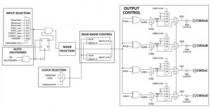
Fig. 1: Simplified block diagram of a complementary waveform generator
Selections
Input sources can be external inputs to the CWGxIN pin or outputs from other internal peripherals. The input source selection bits are used for selecting the input source. The input sources and bit selection settings may vary from device to device.
Some of the available peripherals that can be used as input sources are the comparator, capture compare PWM (CCP), numerically controlled oscillator (NCC) and configurable logic cell (CLC). First, though, the selected peripheral should be configured as the CWG’s input. For devices that have peripheral pin select (PPS), the CWGxIN input pin can be moved to any other pin with the PPS input selection register (xxxPPS). By changing the “xxx” notation in the register name to CWGxIN, any available IO pin can be selected as CWGxIN.
The CWG output can be modified to operate in any of the following modes: half bridge; forward full bridge; reverse full bridge; push-pull; and steering PWM. Mode selection is only available in some devices, where it can be selected by setting the mode selection bits. For example, Fig. 2 shows the output of the CWG in different modes of operation for the Microchip PIC16F161X family.
In half-bridge mode, two output signals are generated as true and inverted versions of the input. In forward and reverse full-bridge modes, three outputs drive static values while the fourth output replicates the input data signal. Toggling a bit in the register switches between forward and reverse mode.
In push-pull mode, the output signals generated are alternating copies of the input. In steering PWM mode, enabling the steering enable bits allows the input event signal to be replicated to any or all of the four CWG outputs. When steering enable bits are cleared, the CWG output signal is determined by the steering data bits. When using a synchronous steering mode, the next rising input event is required before the changes on the steering enable bits take effect. While in non-synchronous steering mode, changes on the steering enable bits take effect on the next instruction cycle.
The reference clock for the dead-band control can be selected from several different clock sources using the clock selection bits. As with the input sources, the available clock sources may vary from device to device.
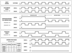
Fig. 2: CWG modes of operation
Dead-band control
Dead-band control provides non-overlapping output signals during half-bridge mode and direction changes during full-bridge mode. The signal prevents the cross conduction of external power switches. The selected clock source is used as a reference to create a delay.
A maximum of a 6bit value can be placed in the rising and falling dead-band counter registers to indicate the count of clock delay periods. When CWGxB goes low, the rising edge dead band starts to count and delays CWGxA for a ten-clock period before it goes high. Likewise, when CWGxA goes low the falling edge dead band starts to count and delays the CWGxB for a ten-clock period before it goes high.
Dead band is timed by counting the clock periods from zero up to the value in its respective count registers. There are instances when this time calculation may not be accurate and this is referred to as time uncertainty, as shown in Fig. 3.
When the rising and falling sources that trigger the dead-band timer come from asynchronous inputs, such as the external input to the CWGxIN pin, it creates an uncertainty in the time.
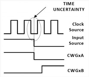
Fig. 3: Time uncertainty
Auto shutdown
Auto shutdown – an active-low operation – can be triggered by a fault event source or by software execution. The fault event source can be selected using the auto-shutdown control register.
When the selected fault event goes low, the output pin will be in shutdown state. The output pin shutdown state can be selected as forced low, forced high, tri-state or inactive by selecting the auto-shutdown state control bits. Also, setting the shutdown bit of the auto-shutdown control register in software will force the output into shutdown state.
The shutdown state can be held until cleared by software or cleared automatically, which requires enabling auto-restart using the auto-restart enable pin.
Output enable
Each CWG output pin has its own enable control. When an output pin enable bit is cleared, the CWG has no connection to the output pin. When the output enable is set, the override value or active waveform is applied to the pin as per the internal port priority selection.
Output control can be completely disabled by clearing the module enable bit. Output enables are selected in the CWG using the output enable bits. Setting the bit enables the output. By default, the complementary drive is configured as inactive in output while the complimentary drive is configured as active in output.
Some devices let the CWG output be moved from default pins to alternative pins using the alternate pin function. For devices that have PPS, there is no output control available. Instead, each device pin has an individual output selection controlled by the PPS register. When the output is not selected in the PPS register, the peripheral has no connection to the output pin.
Polarity control
Polarity control can be set to invert the output signal and the polarity of each CWG output can be selected independently. When the output polarity bit is set, the corresponding output will become active low. Clearing the output polarity bit configures the corresponding output as active high. Inverting the polarity of the output signal would allow two outputs to produce the exact same signal.
Configuration
Microchip’s MPLAB code configurator (MCC) can be used to configure the CWG module. This user-friendly plug-in tool for the MPLAB X IDE generates drivers for controlling and driving peripherals of PIC microcontrollers based on settings and selections made in the GUI.
Conclusion
The complementary waveform generator found in Microchip’s 8bit microcontrollers provides precise half- and full-bridge control for motor driver applications. There are selectable input sources as well as dead-band and polarity control. It can also provide auto recovery and shutdown.


