


The Swedish semiconductor-equipment company has started a six-month assessment of its advanced patterning process within imec’s NanoIC pilot line.
AlixLabs has begun a six-month evaluation of its Atomic Layer Etch Pitch Splitting technology within the NanoIC pilot line coordinated by imec.
The Swedish company develops semiconductor-manufacturing equipment based on atomic-layer etching. Its APS process is intended to divide nanoscale patterns into smaller features, offering a potential alternative or complement to increasingly complex multiple-patterning flows used in advanced logic and memory manufacturing.
The NanoIC pilot line gives AlixLabs access to imec’s lithography, process-integration and metrology capabilities. The project will assess the technology in an advanced pilot-manufacturing environment rather than solely in the company’s own development facilities.
As semiconductor features shrink, manufacturers must control critical dimensions, edge roughness, overlay and defectivity across a growing number of processing steps. Pattern splitting can increase feature density, but its commercial value depends on whether it can be integrated with acceptable process complexity, throughput and yield.
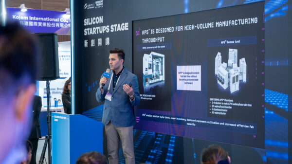
AlixLabs says the work will evaluate how its process performs under conditions relevant to future semiconductor manufacturing. The company’s Sax Forma platform is designed to apply the APS process in equipment intended for industrial use.
The evaluation is a development and validation milestone, not a qualification for volume production. Neither AlixLabs nor imec has disclosed target feature pitch, wafer results, defectivity data, overlay performance, throughput or a customer-production timetable.
For European semiconductor development, the project illustrates how the NanoIC pilot line is being used to move new process technologies from specialist research into a setting where they can be assessed alongside established lithography, metrology and integration flows.
Image credit: AlixLabs / imec