
A 16bit microcontroller and a few external peripherals can be used to create a class D audio amplifier
Class D amplifiers have become popular as an audio amplifier topology due to their high efficiency and low cost. The high current output stage uses binary switches, resulting in low heat generation and power loss. This allows the power supply, heat sink and overall physical size of the amplifier to be reduced.
The typical efficiency of a class D amplifier is more than 90%, as opposed to 50% for a typical class AB amplifier. In an AB design, most of the inefficiency is a result of the output stage devices being required to operate in the linear region. As current flows though the devices, it is converted to heat instead of being delivered to the load.
A single-channel, full-bridge push-pull class D amplifier can be made using only the analogue features of a 16bit microcontroller and a few external components. This leaves the processor available for other applications.
-
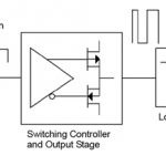
- Figure 1: Block diagram of a class D amplifier
-
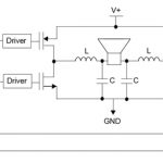
- Fig. 2: Full bridge output circuit diagram
-
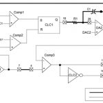
- Fig. 3: Peripheral connections for the PIC24FV16KM202 microcontroller
Class D topology
A class D audio amplifier is essentially a PWM amplifier. The input audio signal is used as the modulation reference for a PWM carrier. The resulting PWM signal drives a higher power output stage, and is filtered to recover the amplified audio. As Fig. 1 shows, there are four main functions in such a device – triangle waveform generator, audio modulation comparator, switch controller and output stage, and low pass filter.
Using a comparator, the analogue audio signal is first compared with a high frequency triangle wave to create a pulse waveform that is directly proportional to the instantaneous values of the audio signal. This results in a digital representation of the analogue signal that can drive the output devices only in on and off states.
Additional logic produces the inverse of the digital signal to drive the complementary switch pair. Next, a switch controller provides signal timing and gate drive voltages for the output devices. The output switches provide voltage gain proportional to the supply voltage, and high current capability to drive the speaker coil. Finally, a low pass filter removes the carrier frequency and recreates the analogue audio signal.
Analogue input
The incoming audio signal needs to be conditioned and filtered before it is compared with the triangle wave. A low pass filter can prevent aliasing, and the level should be limited to below that of the triangle wave. The amplitude of the audio signal may need to be attenuated or amplified to match that of the comparator supplies and triangle wave amplitude.
To improve signal-to-noise ratio, the peak level audio input should be as close to system full scale as possible. Depending on the application and loudspeaker to be driven, it may be beneficial to band limit the input signal. For example, if a small speaker is used that cannot produce tones below 100Hz, the input should be high pass filtered to reduce wasted energy and possible speaker damage.
Power supply
A stable DC power supply is important as it plays a critical role in the performance of the amplifier including gain, THD and noise. Class D amplifiers have little to no power supply noise rejection; any noise or voltage drops from loading will be passed on to the output. Due to the digital nature of the class D design, the power supply has to deliver large current transients each time the output devices switch. The power supply can also be affected by the energy storage elements in the low pass filter and loud-speaker coil.
Output stage
Using a full bridge output stage, as shown in Fig. 2, reduces the power supply’s effect on performance degradation, and can be implemented with a single rail design.
Some dead time is needed to prevent damaging current flow though the switches. Dead time is a delay in driving a switch high due to the capacitive settling effects of the output switch. This prevents both switches from being closed at the same time, effectively shorting V+ to GND. The amount of dead time depends on the switch’s on-off delay, and will affect THD. A full-bridge topology has reduced offset and THD compared with a half bridge, and can be implemented without a feedback circuit. When idle, the PWM duty cycle is 50% and the average voltage on both ends of the speaker coil is V+/2.
Output filter
A typical class D output filter is a second order L-C low pass filter with no resistive components to waste power. The filter cut off frequency should be at least four times lower than the switching frequency of the triangle generator. The application’s speaker nominal impedance will guide the initial values of the inductors and capacitors. However, the speaker coil’s own inductance and capacitance also interact with the filter elements and should be considered in the design.
The power level of the amplifier and resulting current delivered though the filter guides the power rating of the filter elements. Lastly, some designs may have restrictions on radiated emissions (EMI). The filter design, physical location and trace routing need to be considered for best performance.
Implementation
A 16bit microcontroller, such as the PIC24FV16KM202 from Microchip, can have a wide range of analogue and digital peripherals for creating an analogue class D amplifier. The KM device also has configurable internal connections between the peripherals that reduce external PCB routing and free up IO pins for other uses. The FV variant of the family was chosen for its 5V operation, improving the signal-to-noise ratio of the system. Fig. 3 shows the peripherals and connections used for the amplifier.
Op amp OA1 is a buffer for the incoming audio signal. The triangle generator uses a pair of comparators, a configurable logic cell (CLC) module setup as an SR latch and an op amp configured as an integrator. The comparators are wired as a windowed comparator, with thresholds set by DAC1 and the comparator voltage reference.
The windowed comparator’s output is then converted to a square wave using the SR latch, and finally a triangle wave via the integration function of OA1. The triangle wave is fed back to the window comparator completing the self resonator circuit.
Comparator Comp3 creates the pulse waveform by comparing the triangle waveform with the audio input. CLC2 configured as an inverter provides the complement signal for the full bridge topology.
Three comparators are used in the design. Comparators Comp1 and Comp2 function as windowed comparators using the comparator voltage reference and DAC1 to set the voltage threshold levels. Comparator Comp3 compares the audio signal with the triangle wave to create the digital PWM signal.
OA1 acts as a buffer for the incoming analogue audio signal. It is set up as a voltage follower using the selectable internal connection from the output to the inverting input. Optionally, OA1 can be set up as a filter with or without gain. OA2 is used in the triangle generator as an integrator, with its output fed back to the window comparator to create an oscillator.
The digital-to-analogue converters (DACs) are used in a static state to provide a programmable DC voltage level for the triangle generator. DAC1 is internally connected to Comp1’s non-inverting input as the upper voltage threshold of the window comparator. DAC2 is internally connected to OA2’s non-inverting input and used to set the DC bias level at 2.5V (V+/2).
The CLCs provide digital logic for the triangle wave generator and digital output. CLC1 is configured as an RS flip-flop to create a single square wave from the window comparator’s outputs. CLC1’s inputs are internally connected to the comparator outputs. CLC2 is set up as an inverter to create a complementary PWM signal for the low side switches.
Conclusion
The microcontroller’s wide range of analogue and digital peripherals allows it to be used to create a complete class D amplifier. The internal connections between peripherals reduce the pin count needed for implementation, leaving the IO pins available for other uses. Using the peripherals instead of discrete components to realise a Class D design reduces PCB area and overall cost.
