USC researchers have demonstrated a two-terminal selector built from five stacked two-dimensional layers. With nonlinearity above 10 million, endurance exceeding one trillion switching cycles and response times below 20 ns, the device offers a possible way to suppress unwanted currents in dense memory arrays. Scaling the structure to industrial wafer production, however, remains an open challenge.
The difficulty in building denser memory is not always storing a bit in a smaller device. It is often reaching the right cell, reading or updating its state, and preventing current from passing through neighbouring cells on the way. That problem becomes increasingly difficult as memory arrays grow and their wiring becomes more closely packed.
In a study published in Nature Electronics in September 2026, researchers led by Professor J. Joshua Yang at the University of Southern California (USC) demonstrated a new two-terminal selector using five stacked layers of van der Waals materials. A selector is an access device, not a memory cell: it blocks current at low bias and permits much greater current when an appropriate voltage is applied to access the cell.
The reported results are striking: nonlinearity above 10^7, endurance greater than 10^12 switching cycles, and a switching time below 20 nanoseconds. Together, these figures suggest a route to more effective access devices for highly integrated and potentially three-dimensional memory architectures. They were measured in research devices, not in a commercial memory chip or a fully scaled memory array.
One candidate architecture for high-density memory is the crossbar, a grid of intersecting conductors with a memory element at each crossing. Crossbars use chip area efficiently and can, in principle, be stacked vertically. Their simplicity, however, creates an electrical problem: when a selected cell is read, alternative paths through unselected cells can also conduct. These sneak currents reduce the read margin and may raise power consumption.
The issue is particularly relevant to resistive memories, including RRAM, in which information is encoded by different resistance states. Current leaking through other paths can make a high-resistance cell difficult to distinguish from a low-resistance one.
A conventional solution places an access transistor alongside each memory device, creating a one-transistor/one-resistor (1T1R) cell. The transistor offers strong current control but consumes area and complicates dense vertical integration. Another approach is a one-selector/one-resistor (1S1R) cell using a compact, two-terminal access element.
That selector must remain highly resistive under the partial voltages applied to unselected cells, yet conduct sufficient current at the full selected-cell voltage. The crucial property is a strongly nonlinear current-voltage characteristic: a relatively small change in bias produces a very large change in current. High nonlinearity is valuable, but not sufficient on its own. A useful selector must also support practical operating voltages and adequate on-state current, with reliable operation over repeated cycles.
USC’s device draws on the distinctive interfaces of van der Waals materials. Bonds within each atomically thin layer are strong, while the layers interact more weakly with one another. Different two-dimensional crystals can therefore be stacked to form an exceptionally thin heterostructure with a deliberately engineered electronic energy profile.
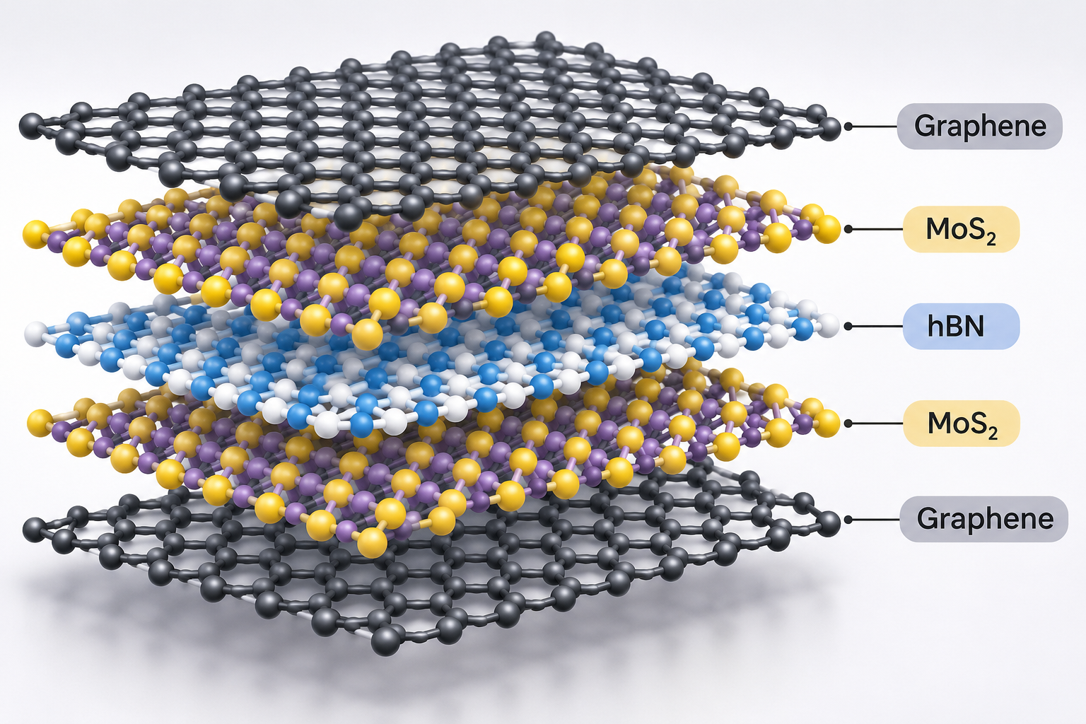
The five functional layers are arranged vertically: graphene, molybdenum disulfide (MoS2), a central tunnelling barrier, a second MoS2 layer, and an upper graphene electrode. The researchers examined two central barrier materials, hexagonal boron nitride (hBN) and gallium sulfide (GaS). Graphene serves as a conducting layer, while the MoS2 layers and the central material shape the barrier electrons must cross.
In quantum tunnelling, an electron has a finite probability of crossing an energy barrier even when it lacks the energy required to pass over it classically. That probability is highly sensitive to the barrier’s height and width. Under low bias, the engineered structure suppresses electron flow. As the applied voltage increases, both the effective height and width of the graded barrier change, sharply raising tunnelling probability and current.
This is distinct from switching mechanisms that depend on the movement of ions or the repeated formation of conductive filaments. In the selector, the switching action relies on electronic transport across the barrier rather than creating and breaking a physical path on each cycle. That may remove certain wear mechanisms, but it does not eliminate interface defects, thermal effects or possible damage under strong electric fields.
Image: Schematic illustration of a five-layer selector structure combining graphene, MoS2 and a central tunnelling barrier. Illustration based on the USC research published in Nature Electronics (2026). Image credit: Illustration supplied with the New-Tech Magazine layout; confirm original artwork ownership and reuse rights before publication.
The team compared devices built with the two barrier materials. The headline performance figures should not be treated as though every value came from one identical device configuration: the material choice influences the operating point and the trade-offs.
| Barrier | Reported result | Parameter |
| hBN | > 10^7 | Nonlinearity |
| hBN | > 10^12 cycles | Switching endurance |
| hBN | < 20 ns | Switching time |
| GaS | 2.5 V | Operating voltage |
| GaS | > 10^6 | Nonlinearity |
Nonlinearity above ten million indicates a sharp separation between current at the selected operating bias and current under a lower bias, at the measurement points used in the study. It is not the on/off resistance ratio of a memory cell: the selector itself does not store information.
Endurance beyond one trillion switching cycles is important for an access device that may be activated whenever a cell is addressed. It demonstrates stability under the reported test conditions, not the lifetime of a complete memory subsystem. Likewise, a response below 20 ns describes the selector, not the full read or write latency of a memory array. Peripheral circuitry, storage-element dynamics, line resistance and parasitic capacitance all add to the system-level timing budget.
The GaS-based design provided operation at 2.5 V with nonlinearity above one million, illustrating how changing the central barrier can tune the device characteristics. The research also reports relatively limited temperature dependence and low variability among tested devices. Both properties matter for large arrays, where cumulative leakage and device spread can erode operating margins.
A central engineering trade-off remains. Very low off-state leakage is useful, but the on-state current must still be high enough for the storage element to be read or programmed. Reducing a barrier to carry more current can also increase unwanted conduction. The graded tunnelling barrier is promising precisely because its energy profile may offer more freedom to balance these opposing requirements.
Beyond measuring standalone selectors, the researchers demonstrated combinations described as 1S1R and 1S1C. In the 1S1R configuration, the selector was connected in series with a hafnium-oxide-based (HfOx) resistive memory device. This shows how the access element can regulate current in a circuit containing an actual storage device.
In the 1S1C configuration, the selector was coupled to a capacitor to examine controlled charging and discharging. This offers an experimental route to evaluating an access element with charge-storage structures. It is not a demonstration of a commercial DRAM cell, nor does it establish data-retention times, refresh behaviour or the performance of an integrated volatile-memory array.
The 1S1R result should be interpreted with the same care. A series-connected research device is not equivalent to a large working crossbar. In an extensive array, wire resistance, parasitic capacitance, voltage division and aggregate sneak currents from many devices become decisive. Validation of dense memory operation will require access tests across many cells under realistic read and write conditions.
The same atomic-scale dimensions that make the selector attractive present a formidable manufacturing challenge. Tunnelling depends exponentially on barrier width; even slight variations in layer thickness, contamination or local interface structure can produce significant electrical differences. Layer uniformity is therefore not merely a geometric target. It is essential to obtaining consistent current-voltage characteristics across devices.
According to USC, the research devices are still assembled manually. Uniform fabrication across industry-standard 300 mm wafers has not been demonstrated. Low device-to-device variability in a laboratory sample is encouraging, but it does not establish the yields, throughput or reproducibility needed for volume manufacturing.
Another hurdle is compatibility with multilayer memory processing. Researchers will need to assess whether the heterostructures survive subsequent thermal steps, how their interfaces behave after integration, and whether they can fit into back-end-of-line process flows. Long-term reliability under electric-field stress, varying temperature and repeated simultaneous operation must also be established.
For device engineers, the significance of the USC work lies in its demonstration that a deliberately shaped, atomic-scale energy barrier can combine high nonlinearity, fast electronic switching and strong cycling endurance. If the approach can be reproduced at wafer scale and integrated into large arrays, it may contribute to denser memories, including three-dimensional architectures. For now, it is a compelling selector research result, not a production-ready memory technology.
Hefei Liu et al., Nature Electronics, 7 September 2026. DOI: 10.1038/s41928-026-01704-2.
USC Viterbi School of Engineering, “A Tiny Gatekeeper Could Keep AI on Your Device,” 21 September 2026.
Suggested image caption: Schematic illustration of a five-layer selector structure combining graphene, MoS2 and a central tunnelling barrier. Illustration based on the USC research published in Nature Electronics (2026).
Image header credit: Illustration supplied with the New-Tech Magazine layout; confirm original artwork ownership and reuse rights before publication.
From durable tactile sensors to contact-aware control and learning from demonstration, recent research is addressing…
A long-term silicon agreement points towards a new generation of digital cockpits and driver-assistance systems.…
Teradyne’s Titan HP combines realistic device workloads, per-device junction-temperature control and a traceable stress history,…
Following functional validation of a 22 nm FD-SOI prototype, Fraunhofer is offering a RISC-V and…
Synaptics’ Astra SR200 family combines heterogeneous Arm cores, Torq neural acceleration and package-integrated DRAM to…
Belgian research institute imec has demonstrated a Ge/Si avalanche photodiode combining 100 GHz bandwidth, 1.8…