
- In this interview, Steven Scheer, senior vice president of Advanced Patterning, Process and Materials at imec, highlights challenges and innovations that will mark the field of patterning in the short and longer term.
- He explains how these are driven by the advent of High NA extreme ultraviolet lithography (EUVL), the rise of new memory and logic device concepts, and the need to reduce the environmental impact of IC manufacturing.
How do you see the field of lithographic patterning evolving over the next two years?
Steven Scheer: “Extreme ultraviolet lithography (EUVL) entered high volume production in 2019 for advanced logic foundries; and dynamic random-access memory (DRAM) companies are increasingly interested in adopting EUVL as well. This could only happen thanks to the phenomenal dedication and commitment of ASML, who pushed the limits of technology far beyond what many people believed possible. The next evolution is the introduction of High NA (0.55NA) EUVL to enable half-pitch imaging down to 8nm.
The next evolution is the introduction of High NA (0.55NA) EUVL to enable half-pitch imaging down to 8nm.
To support the introduction of High NA EUVL, imec and ASML are setting up a High NA EUV Lab to serve the early development needs of the High NA chip manufacturers. At the same time, we are working with the broader patterning equipment and materials supplier ecosystem to enable access to the High NA Lab and prepare EUV resist material, underlayer, dry etch, photomask, resolution enhancement techniques (RET) and metrology technologies.”
What do you see as the key priorities in the introduction of High NA?
“Obviously, the first priority is the availability of the High NA tool. ASML and Zeiss are making phenomenal progress to integrate all modules and optical components. And although a lot of the groundbreaking solutions on process related aspects have been developed for the introduction of low NA EUV, further evolutions will be needed to effectively introduce High NA EUV. In addition to the High NA tool, EUV photoresist development remains one of imec’s first priorities with our ecosystem partners. The advent of High NA EUVL will further increase resolution and reduce feature sizes, at a reduced depth-of-focus. This of course leads to film thickness downscaling, which requires implementation of new resists and underlayers to optimize EUV absorption and pattern transfer during etch.
EUV photoresist development remains one of imec’s first priorities with our ecosystem partners.
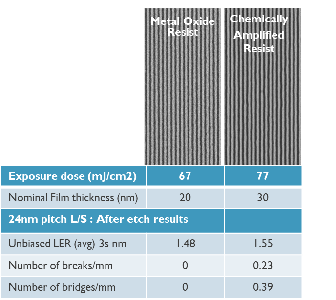
24nm pitch lines and spaces: patterning development for metal-oxide resist (MOR) and chemically amplified resist (CAR). MOR is showing lower dose, better LER and defectivity, despite the low thickness. Credit: IMEC
Additionally, we need to drive continuous improvement in stochastic roughness and, in the extreme case, even failures in EUV patterned resists – a phenomenon we discovered a few years ago. Historically, the photoresist patterning performance is expressed through the resolution, line-edge roughness (LER) or local-CD-uniformity (LCDU), and sensitivity – otherwise known as the RLS parameters. Today, given the importance attributed to stochastics, patterning performance is assessed already at the early-stage development with a fourth parameter (failure) which reflects the process window dimension limited by the stochastics. We believe the solutions exist to mitigate the stochastics failures induced by the photoresist systems and enlarge the process window, while lowering the dose, and intend to work with our partners to demonstrate these new technologies in the High NA Lab.
The reduction of both feature size and resist thickness will impact the metrology as well. Beside printing performances, the drastic dimension shrink has the potential to negatively impact accuracy and precision and therefore metrology and inspection performances.”
How is imec contributing to overcoming the challenges related to EUV photoresists?
“To address the concerns coming from the chemical stochastics (i.e., stochastics other than shot noise) induced by conventional multi-component blended photoresist systems, novel materials are being developed. Examples are metal containing resists or single-component resists. Imec continues to enable material suppliers to develop new concepts and assess critical issues such as contamination risks and process integration challenges.
Novel High NA EUV resist systems cannot be developed in isolated silos: co-optimization with engineered underlayers, novel hard-masks and highly selective etching processes is required to get the best performance. To address this challenge imec has recently developed a new toolbox to match the resist and underlayers properties. By doing material screening, surface energy matching studies, material physical characterization and interface engineering, spin-on or deposited underlayer films can be developed together with the photoresist to enable EUV patterning scaling with optimized LER, sensitivity, and defectivity.
We have set up a patterning materials characterization infrastructure we call the Attolab as a toolbox to get further insights into the behavior of both the resists and underlayers under EUV exposure.
Furthermore, to accelerate materials development, we have set up a patterning materials characterization infrastructure we call the Attolab as a toolbox to get further insights into the behavior of both the resists and underlayers under EUV exposure. Today the absorption coefficient and layer-resolved structural properties of thin films and stacks can be studied with radiometry and reflectometry, techniques made available for partners in the Attolab.”
24nm pitch lines and spaces: patterning development for metal-oxide resist (MOR) and chemically amplified resist (CAR). MOR is showing lower dose, better LER and defectivity, despite the low thickness.
What other avenues is imec exploring to support next lithography nodes?
“There are several new evolutions ongoing in photomask development. To address the requirement of lowering the EUV exposure dose, masks with low-n absorber are being heavily investigated because they create aerial intensity profiles with high contrast (or NILS) at low exposure dose.
At imec, we are also concerned about wafer stochastics and mask 3D effects (i.e., distortions of the aerial image related to the mask 3D topography). Stochastic failures at wafer level have many sources of which mask variability is one. To address the issue, we study which types of mask variability (incl. different roughness’s) are more prone to increased stochastics at wafer level, with the aim of proposing updated mask and blank specs.
Also, High NA EUVL scanners will use anamorphic lenses, which provide unequal magnification in the x and y directions. This anamorphicity implies field stitching on wafer level to achieve the same wafer field size as other, conventional optical lithography. Wafer field stitching puts more importance at mask level to the quality of the mask field edge and possible mitigation schemes.
Due to the increased importance of a deep understanding of the mask interactions with EUV illumination, at imec, we bring together the full mask R&D ecosystem. Together with our mask and blank suppliers, we support the industrialization of mask innovations (like novel absorbers) and explore mask complexity (like variability or stitching), both in the imec-ASML High NA EUV Lab and through modelling.
Due to the increased importance of a deep understanding of the mask interactions with EUV illumination, at imec, we bring together the full mask R&D ecosystem.
None of these issues are fundamental showstoppers for the introduction of High NA EUVL. However, for a smooth, timely and cost-effective introduction of High NA EUV with maximum performance, it is of key importance to address these challenges proactively and to offer to the key players of the ecosystem an effective collaboration platform. The primary motivation of imec and ASML setting up this High NA EUV lab, built around the first High NA scanner, is to facilitate the fastest possible industry introduction and ramp-up of High NA EUV lithography.”
What other developments will impact the field of patterning in the next two to five years?
“In addition to innovations in EUVL, unique patterning opportunities emerge from the rise of new device concepts for both logic and memory that increasingly make use of the third dimension.
Complementary FET (CFET) is the future device architecture beyond gate-all-around (GAA) nanosheets, exploiting the concept of stacking one FET channel on top of another FET device. The device fabrication requires high-aspect-ratio patterning steps to realize the active part, the gate, source/drain recess, as well as the middle-of-line M0A contact formation. Besides, high amounts of material recess such as metal or dielectric will be imperative. Innovations including bottom-up deposition or area selective deposition (ASD) could play an important role in reducing the process complexity for CFET. Next, to allow CFET-based standard cell scaling from 5-tracks to 4-tracks, the CFET device will likely be integrated with backside power delivery. This new routing scheme will require high-aspect-ratio via opening and self-aligned patterning with good selectivity to the gate spacer.
Unique patterning opportunities emerge from the rise of new device concepts for both logic and memory that increasingly make use of the third dimension.
In the memory space, DRAM currently relies on a narrow, tall capacitor as a bit cell. When scaling the pitch to increase density, the lateral critical dimension (CD) of the capacitor will continue to shrink and the capacitor needs to be made increasingly tall to keep the capacitance constant. That will lead not only to manufacturing problems and yield loss, but we also expect 2D DRAM to hit fundamental material limits. To overcome these issues, various 3D DRAM flows are being considered and key challenges are being addressed at module level. We will likely see the introduction of new materials such as semiconductor oxides, complemented with the use of several high-aspect-ratio etching and lateral recess steps, which are challenging in many ways. Next to that, filling of vertical holes and lateral cavities with liners, dielectrics, and metals are expected to be at least as challenging as today encountered in 3D-NAND-Flash technology.”
Moving on to another topic, as your team conducts all process and materials related research at imec: how does imec contribute to a more sustainable manufacturing?
“Today, IC manufacturing is estimated to account for about 0.1 percent of global emissions. However, due to the growing complexity of advanced technology nodes, CO2 emissions associated with manufacturing logic technologies are expected to double in the next 10 years. At the same time, the total volume of wafers produced is projected to grow by ~eight percent annually. If we do nothing, emissions associated with IC manufacturing will quadruple in the next decade. According to the Paris agreement, all industry sectors should cut their emissions in half every decade. In other words, in the “do-nothing” scenario, our industry will be off target by a factor eight.
That’s why sustainability is a key pillar of imec’s research. We launched our sustainable semiconductor technologies and system (SSTS) program, gathering the supply chain to jointly target net-zero emissions for chip manufacturing. To quantify the environmental impact of a generic high-volume semiconductor fab, we are building a virtual fab, called imec.netzero. The developed models are continuously benchmarked and validated through partnerships with equipment and material suppliers.
At the upcoming SPIE Advanced Lithography and Patterning conference, we will present a quantitative assessment of the impact of patterning on carbon emission during advanced IC manufacturing. High-impact areas have been identified and targeted for solutions in our actual fab. Examples include reduced use of fluorinated etch gases, reduced water use, recycling of rare materials, recovery of hydrogen, and lower dose lithography processes.
We will present a quantitative assessment of the impact of patterning on carbon emission during advanced IC manufacturing.
Addressing environmental impact while developing future technologies may seem like a difficult and daunting task. It is. But we can do it. Our industry is known for its creativity and innovation, and we have now added one more development imperative: reduced environmental impact.”

About Steven Scheer
Steven Scheer was appointed as senior vice president of Advanced Patterning, Process and Materials (APPM) at imec in 2022, after joining imec as the vice president of APPM in 2019. His responsibilities include patterning, unit process and new materials development for logic, memory, photonics, and 3D integration. Prior to that, he was an account technology director with Tokyo Electron Ltd. (TEL), responsible for customers in the Portland OR area. He worked at TEL for 13 years where he was responsible for R&D in patterning and cleans, including management roles in the US as well as at TEL’s factory in Kumamoto Japan and with the corporate R&D organization in Tokyo. He began his research career at IBM in Fishkill NY, working on 90 and 65 nm patterning development. He holds a Ph.D. in Chemical Engineering from the University of Texas at Austin.
Credit: Imec
