
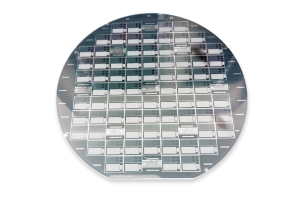
Search for the Next (SFN), developers of the Bizen wafer process, Zpolar transistor and Zpolar Tunnel Logic (ZTL), today announced the WaferTrain network of foundries that is equipped with the Bizen® wafer process and with capacity available now to build ICs that are equivalent to 180nm CMOS devices, yet are half the price and on short leadtimes.
Explains David Summerland, CEO of SFN: “Design engineers and purchasers want to pay less for their ICs and have them now rather than on long leadtimes. But semiconductor makers have limited capacity. By installing our ITM180 process node infrastructure, semiconductor foundries could easily offer their customers savings of 50% on the price of a device. And halve leadtime. If the original device maker is not ready to shift to Bizen, then SFN can replicate the CMOS chip in question and produce an equivalent Bizen device that offers pin-for-pin functionality and performance on the WaferTrain lines.
Bizen applies quantum mechanics to any wafer process technology. The Bizen wafer process is used to build Zpolar Transistors with Zpolar® Tunnel Logic (ZTL). Bizen ZTL chips require fewer processing layers than CMOS, enabling complex devices to be manufactured in large-geometry fabs around the world. So, a 180nm fab using ITM35 Bizen can deliver ZTL chips with the equivalent performance of 35nm CMOS using ten times fewer process steps than an actual 35nm CMOS process. “This decrease in complexity is enough to allow IC makers to slash prices and leadtimes for customers”, adds Summerland.
Although a new technology, the Bizen process can run on standard silicon process technologies using standard CMOS processing equipment. SFN has produced ‘gold standard’ test wafers, which have been characterized, put into a JMP data book and used to produce SPICE models which run in the Cadence design environment, and matches the results from the Synopsis wafer process flow. Last month, SFN released four ITM process nodes: ITM180 which can deliver ZTL chips with the performance of 180nm CMOS using one micron equipment; ITM35 which enables 35nm CMOS-equivalent ICs to be made in 180nm process node fabs; ITM5 which enables 5nm CMOS performance from 28nm steppers, and ITMSubnm which means that current state-of-the-art 3nm fabs will be able to deliver incredible sub-nm, Angstrom-level capabilities.
“We will release ZTL demonstrators in Q1 2023”, concludes Summerland. “These will have real, packaged chips so people can see the final proof of our technology”.
Bizen is patent-protected and is developed in the UK by Search For The Next (SFN). For more details about Bizen, ZTL and SFN, please visit https://www.wafertrain.com/blog, or join in the discussions at https://www.wafertrain.com/discussions, or on social media:
https://www.linkedin.com/company/wafertrain
https://twitter.com/wafertrain
https://www.instagram.com/wafertrain/
