

Introduction
The increasing volume of data collected, communicated, and stored in everything from 5G to industrial applications has expanded the performance limits of analog signal processing devices, some into the gigasamples per second. As the pace of innovation never slows, the next generation of electronics solutions will lead to further shrinking in solution volumes, increasing power efficiency, and greater demand for better noise performance.
One might assume that the noise produced in the various power domains—analog, digital, serial digital, and digital input-output (I/O)—should be simply minimized or isolated to achieve optimum dynamic performance, but chasing the absolute minimum in noise can be a study in diminishing returns. How does a designer know when noise performance of a supply or supplies is sufficient? A good start is to quantify the sensitivity of devices so that the power supply spectral output can be matched to the domain. Knowledge is power: it can greatly help in design by, namely, avoiding over-engineering and thus saving in design time.
This article gives an overview of how to quantify the power supply noise sensitivity of the loads in signal processing chain, and how to calculate the maximum acceptable power supply noise. Measurement setups are also discussed. We finish by touching on some strategies to meet power domain sensitivity with realistic power supply noise requirements. Subsequent articles in this series will dive deeper into the details of optimizing power distribution networks (PDNs) for ADCs, DACs, and RF transceivers.
Understanding and Quantifying Signal Processing Load Sensitivity to Power Supply Noise
The first step in power supply optimization is to investigate the true sensitivity of analog signal processing devices to power supply noise. This includes understanding the effects of power supply noise to key dynamic performance specifications, and characterization of power supply noise sensitivity—namely, the power supply modulation ratio (PSMR) and power supply rejection ratio (PSRR).
PSMR and PSRR are good supply rejection characteristics, but alone they are insufficient to determine how low the ripple should be. This article demonstrates how to establish a ripple tolerance threshold or maximum allowable power supply noise using PSMR and PSRR. Matching this threshold to the power supply spectral output is the basis in designing an optimized power system design. An optimized power supply will not degrade the dynamic performance of each analog signal processing device if power supply noise remains below its maximum specification.
Effects of Power Supply Noise on Analog Signal Processing Devices
The effects of power supply noise on signal processing devices should be understood. These effects can be quantified by three measured parameters:
- Spurious-free dynamic range (SFDR)
- Signal-to-noise ratio (SNR)
- Phase noise (PN)
Understanding the effects of power supply noise on these parameters is the first step to optimizing the power supply noise specification.
Spurious-Free Dynamic Range (SFDR)
Power supply noise can be coupled into the carrier signal of any analog signal processing system. The effect of power supply noise depends on its strength relative to that of the carrier signal in the frequency domain. One measure is SFDR, which represents the smallest signal that can be distinguished from a large interfering signal—specifically, the ratio of the amplitude of the carrier signal to the amplitude of the highest spurious signal, regardless of where it falls in the frequency spectrum, such that:
SFDR = spurious-free dynamic range (dB)
Carrier signal = rms value of the carrier signal amplitude (peak or full scale)
Spurious signal = rms value of the highest spur amplitude in the frequency spectrum
Figure 1. An AD9208 high speed ADC’s SFDR using (a) a clean power supply and (b) a noisy power supply.
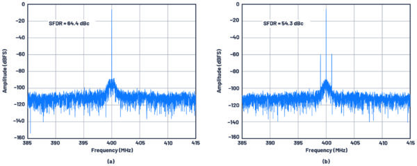
SFDR can be specified with respect to full scale (dBFS) or with respect to the carrier signal (dBc). Power supply ripple can produce unwanted spurs by coupling into the carrier signal, which degrades SFDR. Figure 1 compares the SFDR performance of the AD9208 high speed ADC when powered by a clean vs. a noisy power supply. In this case, power supply noise degrades the SFDR about 10 dB when a 1 MHz power supply ripple appears as modulated spurs beside the carrier frequency in the fast Fourier transform (FFT) spectrum output of the ADC.
Signal-to-Noise Ratio (SNR)
While SFDR depends on the highest spur in the frequency spectrum, the SNR depends on the total noise within the spectrum. SNR limits the capability of an analog signal processing system to see low amplitude signals and is theoretically limited by a converter’s resolution in the system. SNR is mathematically defined as the ratio of the carrier signal level to the sum of all noise spectral components, except the first five harmonics and dc where:
SNR = signal-to-noise ratio (dB)
Carrier signal = rms value of the carrier signal (peak or full scale)
Spectral noise = rms sum of all noise spectral components excluding the first five harmonics
A noisy power supply can contribute to the decrease of SNR by coupling at the carrier signal and adding noise spectral components in the output spectrum. As shown in Figure 2, the SNR of the AD9208 high speed ADC decreases from 56.8 dBFS to
51.7 dBFS when a 1 MHz power supply ripple produces spectral noise components in the FFT output spectrum.
Phase Noise (PN)
Phase noise is a measure of the frequency stability of a signal. Ideally, an oscillator should be able to produce a specific set of stable frequencies over a specific time period. However, in the real world, there are always small, unwanted amplitude and phase fluctuations present on the signal. These phase fluctuations, or jitter, can be seen spreading out on either side of the signal in the frequency spectrum.
Phase noise can be defined in several ways. For the purposes of this article, phase noise is defined as single sideband (SSB) phase noise, a commonly used definition, which uses the ratio of the power density of an offset frequency from the carrier signal to the total power of the carrier signal where:
SSB PN = single sideband phase noise (dBc/Hz)
Sideband power density = noise power per 1 Hz bandwidth at an offset frequency from the carrier signal (W/Hz)
Carrier power = total carrier power (W)
Figure 2. An AD9208 high speed ADC’s SNR using (a) a clean power supply and (b) a noisy power supply.
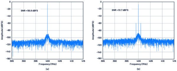
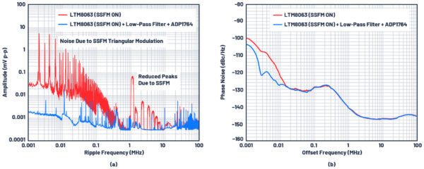
Figure 3. (a) Two different power supplies with significant differences in output noise content. (b) The resulting phase noise performance of the ADRV9009 when powered by those two supplies, respectively.
In the case of analog signal processing devices, voltage noise coupled to the device clock through the clock supply voltage produces phase noise, which in turn affects the frequency stability of the internal local oscillator (LO). This widens the scope of LO frequency in the frequency spectrum, increasing the power density at the corresponding offset frequency from the carrier, in turn increasing phase noise.
Figure 3 shows the comparative phase noise performance of the ADRV9009 transceiver when powered by two different power supplies. Figure 3a shows the noise spectra of the two supplies, and Figure 3b shows the resulting phase noise. Both power supplies are based on the LTM8063 µModule® regulator with spread spectrum frequency modulation (SSFM) on. The advantage of SSFM is that it improves noise performance at the converter’s fundamental switching frequency and its harmonics by spreading the fundamental over a range of frequencies. This can be seen in Figure 3a—note the relatively wide noise peaks at 1 MHz and its harmonics. The trade-off is that the frequency of SSFM’s triangular wave modulation produces noise below 100 kHz—note the peaks starting around 2 kHz.
The alternate power supply adds a low-pass filter to suppress noise above 1 MHz, and an ADP1764 low dropout (LDO) postregulator to reduce the overall noise floor, particularly below 10 kHz (mostly SSFM-induced noise). The overall improvement in power supply noise due to the additional filtering results in enhanced phase noise performance below the 10 kHz offset frequency, as seen in Figure 3b.
Power Supply Noise Sensitivity of Analog Signal Processing Devices
The sensitivity of the load to power supply ripple can be quantified by two parameters:
- Power supply rejection ratio (PSRR)
- Power supply modulation ratio (PSMR)
Power Supply Rejection Ratio (PSRR)
PSRR represents the ability of the device to attenuate the noise on the power supply pin over a range of frequencies. In general, there are two types of PSRR: static (dc) PSRR and dynamic (ac) PSRR. DC PSRR is used as a measure of change in the output offset caused by the variation in the dc power supply voltage. This is a minimal concern, as power supply systems should provide a well-regulated dc voltage to the load. AC PSRR, on the other hand, represents the ability of a device to reject ac signals in the dc power supply over a range of frequencies.
AC PSRR is determined by injecting a sine wave signal at the power supply pin of the device and observing the error spur that appears on the noise floor of the data converter/transceiver output spectrum at the injection frequency (Figure 4). AC PSRR is defined as the ratio of the measured amplitude of the injected signal to the corresponding amplitude of the error spur on the output spectrum where:
Error spur = spur amplitude seen in the output spectrum due to the injected ripple Injected ripple = sine wave amplitude coupled and measured at the input supply pin
Figure 4. Error spur at the output spectrum of analog signal processing devices due to power supply ripple.
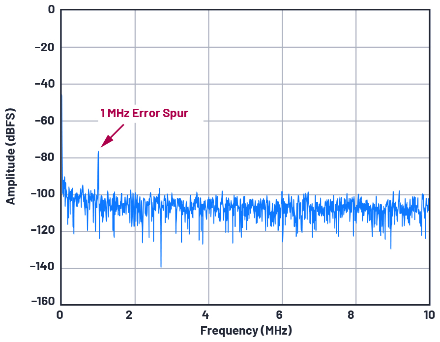
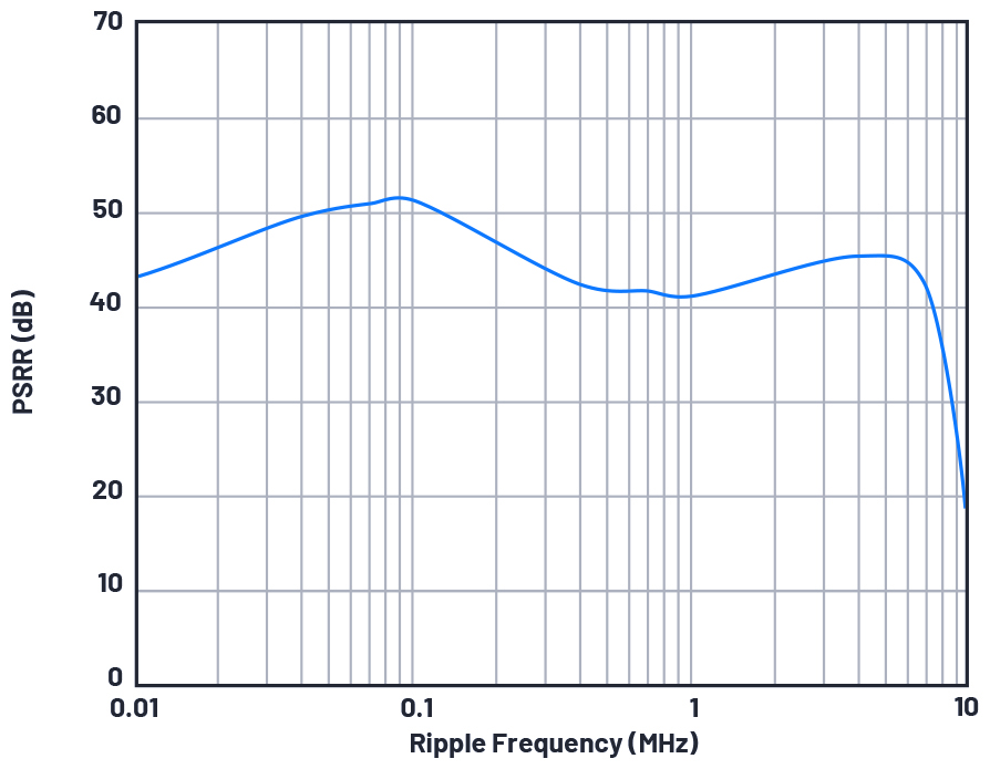
Figure 5 shows the block diagram of a typical PSRR setup. Using the AD9213 10 GSPS high speed ADC as an example, a 1 MHz, 13.3 mV p-p sine wave is actively coupled at the 1.0 V analog supply rail. A corresponding 1 MHz digitized spur appears above the –108 dBFS FFT spectrum noise floor of the ADC. The 1 MHz digitized spur is –81 dBFS, corresponding to a peak-to-peak voltage of 124.8 μV in reference to the analog input full-scale range of 1.4 V p-p. Calculating the ac PSRR at 1 MHz using Equation 4 yields an ac PSRR of 40.5 dB at 1 MHz. Figure 6 shows the ac PSRR of AD9213 for the 1.0 V AVDD rail.
Figure 5. Simplified block diagram of a PSRR/PSMR test setup.
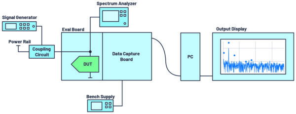
Figure 6. AD9213 high speed ADC ac PSRR for a 1.0 V AVDD rail.
Power Supply Modulation Ratio (PSMR)
PSMR affects analog signal processing devices differently than PSRR. PSMR shows the sensitivity of a device to power supply noise when it modulates with an RF carrier signal. The effect can be seen as a modulated spur around the carrier frequency applied to the device and appears as the carrier sideband.
Power supply modulation is achieved by combining the input ripple signal with a clean dc voltage using a line injector/coupling circuit. Supply ripple is injected as a sine wave signal from the signal generator to the power supply pin. The sine wave modulated into the RF carrier creates sideband spurs with offset frequency equal to the sine wave frequency. The level of the spurs is affected by both the sine wave amplitude and the sensitivity of the device. A simplified PSMR test setup is the same as that of PSRR as shown in Figure 5, but the output display is focused on the carrier frequency and its sideband spurs as shown in Figure 7. PSMR is defined as the ratio of the injected ripple amplitude of the power supply to the modulated sideband spur amplitude around the carrier where:
Modulated spur = spur amplitude at the sideband of the carrier frequency due to the injected ripple
Injected ripple = sine wave amplitude coupled and measured at the input supply pin
Figure 7. Modulated sideband spurs in the carrier signal due to power supply ripple.
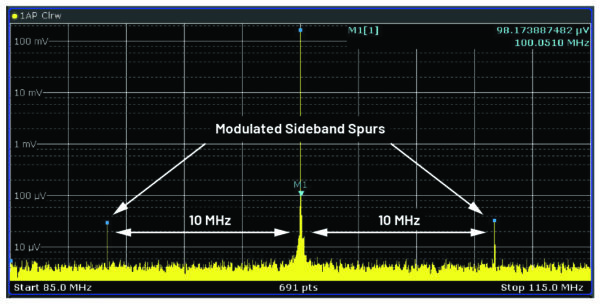
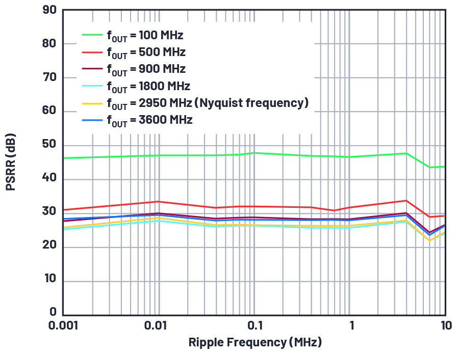
Consider the AD9175 12.6 GSPS high speed DAC operating with a 100 MHz carrier, and a 10 MHz supply ripple of about 3.05 mV p-p actively coupled at the 1.0 V AVDD rail. A corresponding 24.6 μV p-p modulated spur appears in the sideband of the carrier signal with offset equal to the frequency of the supply ripple of about 10 MHz. Calculating the PSMR at 10 MHz using Equation 5 yields 41.9 dB. Figure 8 shows the AD9175 1.0V AVDD rail PSMR for channel DAC0 at various carrier frequencies.
Figure 8. AD9175 high speed DAC PSMR for a 1.0 V AVDD rail (Channel DAC0).
Determining Maximum Allowable Power Supply Ripple
PSMR can be combined with a powered device’s reference threshold to determine the maximum allowable voltage ripple on each of the power supply domains of an analog signal processing device. The reference threshold itself can be one of several values representing the allowable spur level (as caused by power supply ripple) that the device can tolerate without significantly affecting its dynamic performance. This spur level can be the spurious-free dynamic range (SFDR), a percentage of least significant bit (LSB) or output spectrum noise floor. Equation 6 shows the maximum allowable input ripple (VR_MAX) as a function of PSMR and the measured noise floor of each device where:
VR_MAX = the maximum allowable voltage ripple on each of the power supply rails before producing spur in the output spectrum noise floor
PSMR = the noise sensitivity of the power supply rail of interest (in dB)
Threshold = a predefined reference threshold (for the purposes of this article, the output spectrum noise floor)
For example, the output spectrum noise floor of AD9175 is about 1 μV p-p. The PSMR at 10 MHz ripple for the 1800 MHz carrier is about 20.9 dB. Using Equation 6, the maximum allowable ripple in the device supply pin that it can tolerate without degrading its dynamic performance is 11.1 μV p-p.
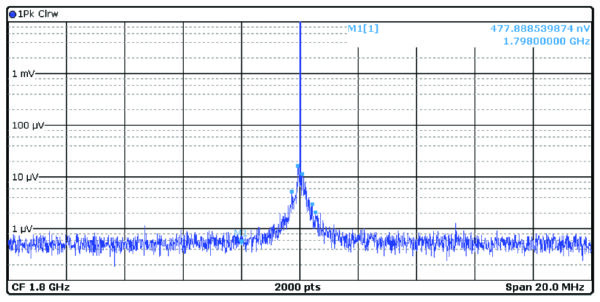
Figure 9 shows the combined results of the spectral output of the LT8650S step-down Silent Switcher® regulator (with and without an output LC filter) and the maximum allowable ripple of AD9175 for the 1.0 V AVDD rail. The regulator spectral output contains spurs at the fundamental switching frequency and its harmonics. The LT8650S directly powering the AD9175 produces a fundamental exceeding the maximum allowable threshold, resulting in modulated sideband spurs in the output spectrum, as shown in Figure 10. Simply adding an LC filter reduces the switching spurs below the maximum allowable ripple, as shown in Figure 11.
Figure 9. LT8650S power supply spectral output vs. the maximum allowable voltage ripple at the 1.0 V AVDD rail.
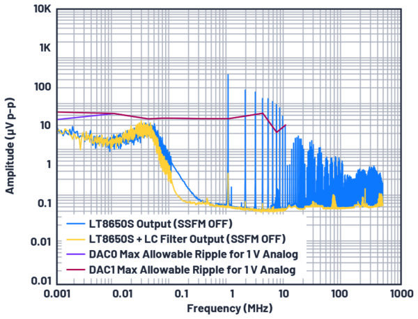
Figure 10. AD9175 DAC0 output spectrum at 1800 MHz carrier frequency using the LT8650S dc-to-dc Silent Switcher converter output directly to the AVDD rail.
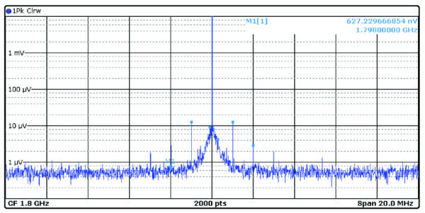
Figure 11. AD9175 DAC0 output spectrum at 1800 MHz carrier frequency using an LT8650S with LC filter power supply.
Conclusion
The superior dynamic performance of high speed analog signal processing devices can easily be undercut by power supply noise. A thorough understanding of the sensitivity of the signal chain to power supply noise is necessary to avoid performance degradation of the system. This can be determined by establishing a maximum allowable ripple—vital to designing the power distribution network (PDN). When the maximum allowable ripple threshold is known, various approaches in designing an optimized power supply can be applied. A good margin from the maximum allowable ripple is an indication that the PDN will not degrade the dynamic performance of high speed analog signal processing devices.
References
Delos, Peter. “Power Supply Modulation Ratio Demystified: How Does PSMR Differ from PSRR?” Analog Devices, Inc., December 2018.
Delos, Peter and Jarrett Liner. “Improved DAC Phase Noise Measurements Enable Ultralow Phase Noise DDS Applications.” Analog Dialogue, Vol. 51, No. 3, August 2017.
“The Essential Guide to Data Conversion.” Analog Devices, Inc.
Jayamohan, Umesh. “Powering GSPS or RF Sampling ADCs: Switcher vs. LDO.” Analog Devices, Inc., November 2015.
Limjoco, Aldrick, Patrick Errgy Pasaquian, and Jefferson Eco. “Silent Switcher μModule Regulators Quietly Power GSPS Sampling ADCs in Half the Space.” Analog Devices, Inc., October 2018.
Naeem, Naveed and Samantha Fontaine. “Characterizing the PSRR of Data Acquisition μModule Devices with Internal Bypass Capacitors.” Analog Dialogue, Vol. 54, No. 3, July 2020.
About the Author
Pablo Perez Jr. joined Analog Devices as an ADEF senior applications engineer in May 2019. His work experiences include modification and evaluation of standard switch-mode power supplies for different applications (industrial, telecommunications, medical, military) and design verification and sample evaluation of linear regulators, switching regulators, and power management ICs. Pablo graduated with a B.S. in electronics and communications engineering at Manuel S. Enverga University Foundation, Inc., in Lucena City, Quezon, Philippines. He can be reached at pablo.perezjr@analog.com.
About the Author
Patrick Errgy Pasaquian has been at Analog Devices for seven years. He joined ADI in 2014 and works as a senior applications engineer focusing on aerospace and defense (ADEF) power systems. He has handled various engineering roles in applications development, design evaluation, power attached to ADEF signal chains, and customer support through EngineerZone and Who’s Who. He has authored and showcased several papers and projects at the ADI General Technical Conference (GTC), Asia Technical Symposium (ATS), and ADI Philippines Technical Symposium (ADTS). He received his bachelor’s degree in electronics engineering at Central Philippine University in
