


This week, at the International Solid-State Circuits Conference (ISSCC2020), imec, a world-leading research and innovation hub in nanoelectronics and digital technologies, in collaboration with Ghent University demonstrates for the first time a high-speed silicon analog time-interleaver achieving signalling rates up to 100 Gbaud (200Gb/s) at a power consumption of only 700mW using PAM-4 modulation. The demonstrated new architecture is a crucial building block for high-speed optical transceivers in future datacenters.
Over the next few years, datacenters will upgrade their networks to cope with the exploding demand for data consumption. A growing number of optical links interconnects the server racks through a hierarchical network of fiber optical cables. While these links need to be low cost and low power, they require an increase in signaling rate up to at least 100 Gbaud.
Optical transceivers with such high speeds only are achievable with state-of-the-art Indium phosphide (InP) based implementations, but this process comes with a high fabrication cost and a yield that might be too low for large-scale production. CMOS processes are more scalable, but achieve lower speeds due to a limited analog bandwidth. In particular, pushing the bandwidth of the digital-to-analog converter (DAC) beyond 50 GHz is challenging in a CMOS chip.
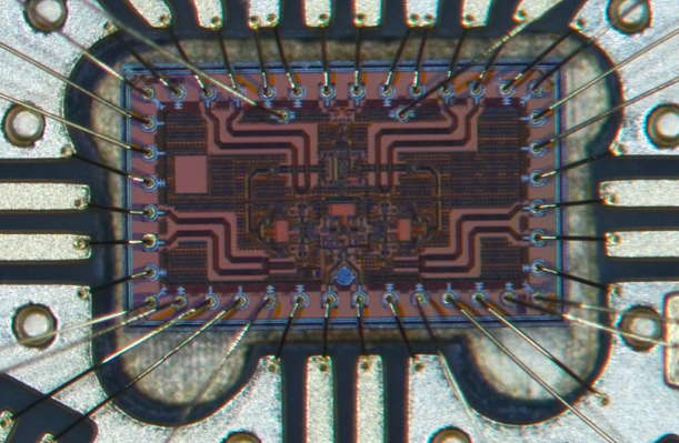
Scientists from IDLab, an imec research group at Ghent University, now managed to achieve a higher bandwidth using a 55nm SiGe BiCMOS technology. On the BiCMOS-chip, where the signal processing is performed, the outputs of four DACs are combined and by time-interleaving four 25 Gbaud streams a 100 Gbaud-signal is created. This is equivalent to a single DAC operating at 100 GS/s (giga-samples-per-second). By using the PAM-4 modulation format, a data rate of 200 Gb/s is obtained. Despite the significant increase in sampling rate, the total power consumption of the prototype stays low (700 mW), which is important given the problem of the rapidly increasing electricity consumption in data centers.
“Compared to other silicon implementations, this new circuit architecture combines a significant increase in baud rate with a lower power dissipation. In addition, the scalable SiGe BiCMOS technology can be implemented at high manufacturing volume, paving the way to cost-effective high-speed optical transceivers for the next-generation data center”, says Guy Torfs (UGent/ imec).
The analog time-interleaver will be demonstrated at the 2020 International Solid-State Circuits Conference. The research was supported by the European H2020 project ICT QAMeleon.
The project QAMeleon has received funding from the European Union’s Horizon 2020 research and innovation programme under grant agreement No 780354.


