

System-technology co-optimization (STCO) – enabled by 3D integration technologies – is seen as a next ‘knob’ for continuing the scaling path. Eric Beyne, imec fellow and program director of imec’s 3D system integration program and Julien Ryckaert, program director 3D hybrid scaling at imec, unravel the STCO principle, open up the 3D technology toolbox and bring up two promising cases: logic on memory, and backside power delivery.
After DTCO comes STCO…
For many years, the semiconductor industry has lived in an era of ‘happy scaling’ – driven by the Law of Gordon Moore. In this era, dimensional scaling alone could provide each new technology generation with the required power-performance-area-cost benefits. But the last 15 years, the chip industry has not been following that happy scaling path anymore. Dimensional scaling started to provide diminishing returns, marking the end of that era.
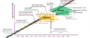
Figure 1: From DTCO to STCO
From the 10nm technology generation onwards, traditional scaling has been complemented by design-technology co-optimization (DTCO), combining expertise from technology as well as from design. In this DTCO era, track height reduction and a growing number of structural scaling boosters have been introduced, allowing to scale standard cells and static random access memories (SRAMs) to an extreme level of compactness. Scaling boosters include, for example, self-aligned gate contact, metal-gate cut and supervia.
But as we move further and look at the benefits of what DTCO can bring at system-on-chip (SoC) level, we can expect a certain saturation – especially when we start considering global access and power delivery to the SoC.
Therefore, for 3nm and beyond technology nodes, we will need to shift focus from scaling at logic cell level towards scaling at system level. Hence, DTCO is evolving into an STCO-oriented approach.
STCO: a clever way of disintegration
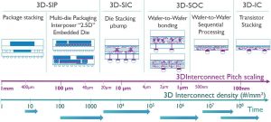
Figure 2: The 3D technology integration landscape
In general, STCO involves the disintegration and reintegration of a SoC. A SoC is composed of various (heterogeneous) sub-systems (functions) that are interconnected by a complex wire scheme. When disintegrating a SoC, it should be decided in a clever way at what level in this wiring interconnect hierarchy the system is cut into different partitions.
But how can this be done? What components belong together, and which should be processed separately? Most often, a trade-off is to be made between the interconnect granularity – the level of granularity at which the different parts of the system will be reconnected – and the technology heterogeneity. For example, if we want to reach a very fine interconnect granularity, we will not be able to reconnect a wide variety in technologies.
After dis-integration, each of these sub-systems can then be designed and processed separately, with the most appropriate technology.
Following this approach, we will move away from a longstanding guiding principle that has been used to make ever more advanced systems-on-chip: the universality of CMOS technology.
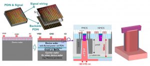
Figure 3: Principle of functional backside power delivery network using
nano-TSV to contact buried power rails through ultra-thin Si device layers.
So far, all the different functions on a chip (including, for example, logic, memory, I/O interfaces, power etc) were hooked onto one and the same CMOS technology platform. Scaling of that CMOS technology has enabled ever more performant systems.
But as SoCs are becoming increasingly more heterogeneous, it will be more advantageous to use a different process technology – which could as well be multi-node variations of one technology – for the different needs of the sub-systems. Memory, for example, does not need to be process-compatible with logic. Or, think about sensors and other analog functionalities that do not really benefit from using ultimately scaled technologies. For these functions, simpler processes and more relaxed lithography can be used.
With this approach, we expect to make even more progress in terms of power, performance, area and cost – offering new scaling opportunities for future electronic systems.
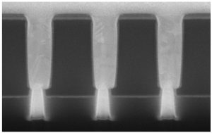
Figure 4: Backside power delivery network: first hardware demonstration
Reintegration: 3D integration technologies to the rescue
After disintegrating the SoC and optimizing the different sub-systems, they need to be reintegrated in a smart way by using one of the available 3D integration technologies.
Different 3D integration technologies can be applied at different levels of the interconnect hierarchy, spanning an exponential scale in interconnect density (i.e. the number of connections per mm2) – from the mm-scale to the nm-scale.
This 3D interconnect technology landscape can be illustrated with the graph below. The graph represents the various 3D integration approaches with respect to the achievable 3D interconnect density and pitch.
At the ‘coarser’ left side of the graph are the technologies that are typically being used if only a limited number of connections is needed between the system’s sub-components. Here, partitioning is done at package level, by stacking packages on top of each other. This system-in-a package (SiP) approach has been illustrated for the case of DRAM stacking. Coarse contact pitches in the order of 400µm can be achieved. As an alternative approach to SiP, multiple die can be integrated in a single package using passive interposers – known as 2.5D integration. This is for example being used for ‘chiplet’ style of manufacturing. Or, one of the many fan-out wafer-level packaging flavours can be applied, which are an attractive solution for mobile applications such as smartphones – as they potentially enable cost-effective wide I/O die-to-die interconnects in small form factors. Many of these techniques use horizontal as well as vertical interconnections.
Higher 3D interconnect densities can be achieved by using die-to-wafer stacking techniques, where finished dies are bonded on top of a fully processed wafer. Dies are interconnected using through-Si vias (TSVs) or microbumps. Imec’s goal is to bring these microbump pitches down, below 10µm.
Next come wafer-to-wafer bonding techniques, enabling true 3D system-on-chips. These are packages in which partitions with varying functions and technologies are stacked heterogeneously, with interconnect pitches in the order of 1µm. Either hybrid wafer-to-wafer bonding or dielectric wafer-to-wafer bonding techniques can be applied.
The highest interconnect density is realized so far by using sequential processes. Ultimately, transistors can be stacked on top of each other, achieving contact pitches as small as 100nm. The true value of these sequential processing is whenever a second layer needs to have a lithography precision of alignment with respect to the bottom layer. An interesting application that can potentially benefit from this precise alignment, is ‘array under CMOS’ – involving splitting up the periphery from the array. This approach could be considered for applications such as imagers or selectors for memory.
An unusual roadmap
It is important to note that this 3D landscape should not be read like a timeline from left to right. There is no single packaging technology that can serve all needs.
Instead, the different 3D integration options exist next to each other, and can even co-exist in one and the same system.
And each option has its own roadmap, with interconnect densities and pitches improving in time. But the choice of what is the best 3D integration technology entirely depends on the application, and on the ‘traffic’ between each element that you partition. It is a collection of technologies that allow a system to be integrated into a much smaller form factor, with optimized performance and power, and at lower manufacturing cost – in support of STCO.
Where logic and 3D meet: two STCO cases
Various functions of a SoC (such as image sensors or memory components) have already been subject to partitioning and reintegration by using one of the available 3D integration technologies. But so far, the logic part of the system has mainly stayed out of this ‘3D picture’. Below, two cases illustrate how this has recently changed: the case of logic on memory, and the case of backside power delivery.
They will show how logic and 3D start to meet in the STCO framework, and how smart partitioning can provide a knob for further CMOS scaling.
In both cases, we consider three key functions of the SoC: logic core, cache memory and storage, and power delivery.
Logic on memory
In traditional systems, a memory array is placed next to the logic core that it supports. This gives an average interconnect line length that depends on both the spacing between the two devices and the bump pitch on the individual die.
Alternatively, functional partitioning and wafer-to-wafer bonding techniques can be used to stack the memory vertically on top of the logic component. The memory can be manufactured in a memory-optimized process on one wafer, and core logic can be manufactured on another.
Benefits of this approach are a potential reduction in die area, and an obvious reduction in footprint. It also allows functional memory (e.g. the level-2 cache) to be positioned in close proximity to the logic it serves, with the average line length being the vertical spacing between the two components. This results in increased performance (interconnect bandwidth) at reduced power consumption.
Backside power delivery
The goal of a power delivery network is to provide power and reference voltage to the active devices on the die. This network is essentially a network of interconnects that is completely separate from the signal network. Traditionally, both the signal and power networks are processed in the wafer’s back-end-of-line – which is at the front-side of the Si wafer.
We can also envision to provide the global power from the backside of the wafer. From there, this network of interconnects can connect to a buried power rail, a scaling booster in the form of a local power rail that is buried in the chip’s front-end-of-line.
In practice, this backside processing can be done by first hooking the CMOS processed wafer onto a carrier using wafer-to-wafer bonding. Then, the wafer’s backside is thinned down with an extreme level of thinning – to about a few 100nm. This allows to expose nm-scale through-Si vias that run from the wafer frontside to the backside and connect them with extremely fine granularity.
By directly delivering power to the standard cells through the backside, the imec team recently demonstrated a 30% area scaling benefit. In addition, implementing the power delivery network in the backside can relieve the frontside (i.e., the back-end-of-line or BEOL) from power routing, which reduces the BEOL complexity. It also improves the supply voltage drop (or IR drop, which is caused by a resistance increase in the back-end-of-line), providing up to 15% performance enhancement.
It is interesting to note that this concept of functional backside processing can be extended beyond power delivery.
One can start thinking of implementing other functions within the wafer’s backside, including, for example, metal-insulator-metal (MIM) capacitors, electrostatic discharge (ESD) devices or indium-gallium-zinc-oxide (IGZO) transistors.
In summary…
With DTCO running out of steam, we are now at the eve of a new age: the era of STCO – where scaling at logic cell level will be complemented by scaling at a global system level. STCO involves the SoC to be disintegrated, and subsequently reintegrated by using one of the available 3D integration technologies. These technologies can be applied at different levels of the 3D interconnect hierarchy, from the package to the die, to the wafer, to the standard cell and even to the transistor level. Two cases – logic on die, and backside power delivery – illustrate how this STCO framework is now also penetrating the logic world – providing further knobs for continuing the scaling path.
 About Julien Ryckaert
Julien Ryckaert received the M.Sc. degree in electrical engineering from the University of Brussels (ULB), Belgium, in 2000 and the PhD degree from the Vrije Universiteit Brussel (VUB) in 2007. He joined imec as a mixed-signal designer in 2000 specializing in RF transceivers, ultra-low power circuit techniques and analog-to-digital converters. In 2010 he joined the process technology division in charge of design enablement for 3DIC technology. Since 2013, he is in charge of imec’s design-technology co-optimization (DTCO) platform for advanced CMOS technology nodes. He is now program director focusing on scaling beyond the 3nm technology node as well as the 3D scaling extensions of CMOS.
 About Eric Beyne
Eric Beyne obtained a degree in electrical engineering in 1983 and the Ph.D. in applied sciences in 1990, both from the Katholieke Universiteit Leuven, Belgium. Since 1986 he has been with imec in Leuven, Belgium where he has worked on advanced packaging and interconnect technologies. Currently, he is imec fellow and program director of imec’s 3D system integration program. He received the European Semi Award 2016 for contributions to the development of 3D technologies.
