LEUVEN, Belgium—Dec. 4, 2017 – At this week’s 2017 International Electron Devices Meeting (IEDM), imec, the world-leading research and innovation hub in nano-electronics and digital technology, reports on multiple key process optimizations for vertically stacked gate-all-around (GAA) silicon nanowire transistors. The optimized CMOS process flow was then used to integrate, for the first time, the GAA nanowire transistors in a functional ring oscillator. This demonstrator shows the enormous promise this technology holds for realizing the sub-5nm technology nodes.
Gate-all-around (GAA) MOSFETs based on vertically stacked horizontal nanowires or nanosheets are promising candidates to succeed FinFETs in sub-5nm technology nodes, thus extending today’s CMOS technology beyond its scaling limits. This innnovative transistor architecture offers a more aggressive gate pitch scaling than FinFETs because it achieves a better electrostatic control. Moreover, in very scaled standard cells where only one fin device is allowed, nanosheets provide more current per footprint than fins, and thus can drive higher capacitive loads. Finally, integrating nanosheet devices with variable widths in a single platform enables power/performance optimization with high granularity.
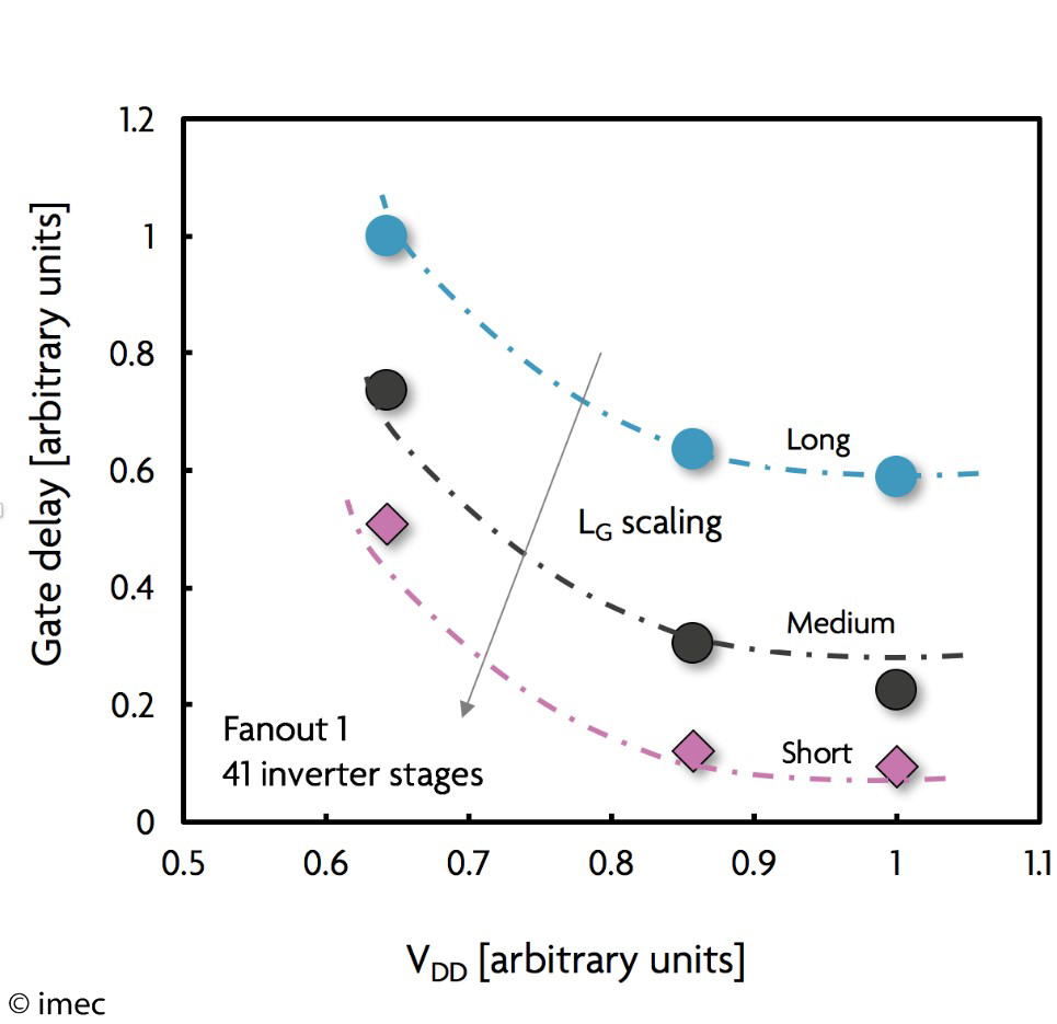
As with every disruptive innovation, this new architecture demands for process optimizations. At IEDM, a team of researchers from imec and Applied Materials demonstrated multiple optimizations for the fabrication of stacked silicon nanowire and nanosheet FETs. The first process optimization is the implementation of a SiN Shallow Trench Isolation (STI) liners which suppresses oxidation-induced fin deformation and improves the shape control of the nanowire or nanosheet. Secondly, SelectraTM etch was used to enable nanowire/nanosheet release and inner spacer cavity formation with high selectivity and without causing silicon reflow. Finally, for the first time, ring oscillator circuits were reported based on stacked silicon nanowire FETs, including dual work function metal gates for threshold voltage control.
At IEDM, imec also presented a study on the reliability of GAA nanowires showing that the degradation mechanisms and their origins are similar as the one in planar devices. The modelling of the degradation including various channel hot-carrier (CHC) modes as well as positive bias temperature instability (PBTI) allows an extrapolation to 10-years lifetime in the full bias space. The obtained safe operation area (SOA) was used to optimize device operation. An extra degradation mechanism that must be taken into account is self-heating, which is very important in such confined structures. Finally, in a study on ESD diodes in sub-7nm GAA nanowire technology nodes, imec proved that the diodes performance is significantly impacted by some of the process options and that optimizations are needed, such as a wrap around contact (WAC) which can increase contact area in a scaled fin pitch and can be combined with GAA.
Imec’s research into advanced logic scaling is performed in cooperation with imec’s key CMOS program partners including GlobalFoundries, Huawei, Intel, Micron, Qualcomm, Samsung, SanDisk/Western Digital, SK Hynix, Sony Semiconductor Solutions, TOSHIBA Memory and TSMC.


