
Abstract
A design based on digital demodulator and JESD204B interface for multiple channel ultrasound receive systems is introduced. The design reduces the data rates and simplifies board routing between the Analog Front End (AFE) and digital processing circuits up to 80%. In addition, the ultrasound system can achieve more design goals, such as utilization of cheaper and less computationally efficient Field Programmable Gate Arrays (FPGA), a software-based beam-former, and higher order multiline processing for real-time 4D and advanced imaging modes.
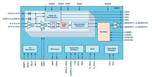
Figure 1. 128-channel ultrasound system block diagram
Introduction
Ultrasonic imaging systems designers must continuously struggle to meet the demand for ever-higher image quality being made by users throughout the medical diagnostics field. One of the key techniques for image quality improvement is to enhance the signal-to-noise ratio of the receiving channel. As the number of receiving channels in a system doubles, the signal-to-noise ratio should improve by 3 dB in theory. Therefore, increasing the number of system channels has become the easiest and most effective method to strengthen the signal-to-noise ratio.
At present, 128-channel has successfully become the mainstream configuration for middle to high level medical ultrasound equipment, and 192 or more channels will become the next trend for premium systems.
With the increase of number of the channels, the data rates between the analog front end (AFE) and back end digital processing section grow proportionally. Higher channel counts also create similar growth in the number of digital circuit device interfaces, the processing power, the costs, and the design complexity of the entire receiver circuit. For example, most ultrasound imaging systems use Radio Frequency (RF) beamforming techniques where the output data rate is entirely determined based on the resolution, sampling rate, and channel numbers of the analog-to-digital converter (ADC). Meanwhile, the Analog Front End (AFE) usually uses Low-Voltage Differential Signaling (LVDS) output interfaces. An octal AFE requires 8 pairs of LVDS data wires plus a pair of data clock and frame clock each. For a system with over 128 channels, there are significant amounts of data and physical connections.
This paper introduces an ultrasound receiving channel design solution based on an octal AFE with digital demodulator interface with ADI’s JESD204B being used as an example. Using this approach effectively resolves the design difficulties caused by the large data rates and complex physical connections of the system as mentioned above.
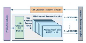
Figure 2. AD9671 functional block diagram
System Architecture
An ultrasound system is composed of a probe (transducer), transmitting circuit, receiving circuit, back end digital processing circuit, control circuit, display module, etc. Figure 1 is the block diagram of a 128-channel ultrasound system transmit/receive path with JESD204B interface.
The digital processing module usually comprises a Field Programmable Gate Array (FPGA) which generates the corresponding waveforms according to the current configuration and control parameters of the system, and the transmit circuit’s driver and the high-voltage circuit then generate a high voltage to excite the ultrasound transduces. The ultrasound transducer is usually made of Piezoelectric Ceramic Transduce (PZT). It converts a voltage signal into an ultrasound wave that enters into the human body while receiving the echoes produced by the body’s bone and tissue.
The incoming echoes are converted into a voltage signal and transmitted to a transmitting/receiving (T/R) switching circuit. The primary objective of the T/R switch circuit is to prevent the high-voltage transmit signal from damaging the low-voltage receive analog front end. The incoming analog voltage signal is amplified and subjected to signal conditioning and filtering before being passed to the AFE’s integrated ADC where it is converted into digital data. The digitized signal is then transmitted through a JESD204B interface to the back end digital parts for the corresponding processing to eventually create the ultrasound image. The receiving channel is composed of a 128 channel T/R switching circuit, 16 octal channel ultrasound AFE elements with a digital demodulator and an FPGA with an JESD204B interface.
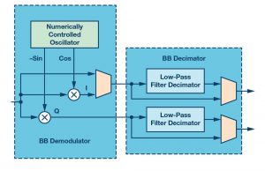
Figure 3. Digital demodulator block diagram
Octal Ultrasound AFE with Digital Demodulator and Interface
The AD9671 octal ultrasound AFE with digital Demodulator and JESD204B interface from Analog Devices (ADI), form the basis of this ultrasound system receiving circuit. It contains eight Variable Gain Amplifier (VGA) channels with a Low Noise Amplifier (LNA), a Continuous Wave (CW) harmonic rejection I/Q demodulator with programmable phase rotation, an Anti-Aliasing Filter (AAF), a 14-bit ADC, a digital demodulator and decimator for data processing and bandwidth reduction, and JESD204B interfaces. Figure 2 is a functional block diagram of the AD9671.
The digital demodulator is composed of a baseband demodulator and baseband decimator. The demodulator down converts the RF signal to a baseband quadrature signal. The excess oversampling is reduced by the decimator. Figure 3 is a block diagram of a digital demodulator.
Interface
The AD9671 digital output complies with the JEDEC Standard JESD204B, Serial Interface for Data Converters. The AD9671 supports single, dual, or quad lane interfaces. It can connect to an FPGA with a maximum data output rate of 5.0 Gbps.
System Design and Application
The receiving circuit design of the AD9671 multi-channel ultrasound system is introduced in this section and the benefits of using digital demodulators and the JESD204B interfaces for the system are analyzed further.
Receive Circuit Design
A 32 channel receive circuit module schematic top diagram is shown in figure 4, which can be designed to verify the feasibility of the system based on the AD9671. With four such modules, a 128 channel receive circuit of an ultrasound system can be configured. This module can be used to perform data capture and processing as well as achieve ultrasonic signal processing and image generation by connecting to an FPGA through a dedicated FMC connector.
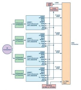
Figure 4. Top-level schematic diagram of the receiving circuit
Digital Demodulator Application Analysis
For a 128 channel ultrasound system, if a 14-bit ADC is utilized with a sampling rate of 40 MSPS, and an RF beamforming algorithm is used, then, the data rates between the ADC output and the beamforming FPGA is 14 * 40 * 128 = 71.68 Gbps.
The benefits of using a digital demodulator are analyzed below.
The baseband demodulator of the RF signal performs quadrature demodulation. It can be achieved by multiplying the digitized RF signal outputted by the ADC with a complex sinusoidal signal , where is the demodulation frequency that can be close to the center frequency of the ultrasound transducer to down-convert the center frequency to around 0 Hz. The output signal is a complex signal that is represented by its I (In phase) and Q (Quadrature phase). The center frequency of the probe and all of the interested frequency bands signals are down shifted to approximately 0 Hz, the unwanted frequency components are filtered out with the filters and decimator to retain the band information that is useful to generate the ultrasound images.
For a probe transducer with a center frequency of 3.5 MHz, after baseband demodulation and decimation, with 16-bit format I and Q data output, the data rate is now 2 (I&Q)* 16-bits * 3.5 MHz* 128 channels = 14.336 Gbps. Compared to the original 71.68Gbps, the data rate is decreased by 80% even with the I and the Q channels outputting simultaneously.
Interface Application Analysis
In terms of current AFE and ADC in multi-channel ultrasound system applications, LVDS has replaced the parallel output interface. However, for the 128-channel or higher ultrasound system, the large amounts of LVDS wire connections for the ADC output is still a headache for the design engineers. With LVDS, there are 10 pairs of wire for one octal AFE in a current ultrasound system. For a 128-channel ultrasound system, 128/8*10=160 pairs of LVDS data and clock wires are required to be connected to the FPGA.
The benefits of using the JESD204B interface are analyzed below.
As the JESD204B uses a 16-bit digital output format and uses 8B/10B encoding, the output data rate for an octal AFE with 14-bit resolution, 40 MSPSADC the sampling rate is 20*40*8=6.4Gbps. The maximum data rate of each lane of the AD9671 JESD204B interface is 5.0 Gbps, so only 2 pairs of data lane are needed to implement an 8 channel AFE data output. So for a 128-channel ultrasound system, only 128/8*2=32 pairs of output data lanes are required as compared to 160 pairs of the LVDS wires; 80% of the physical interface routing is eliminated.
Conclusion
A multi-channel ultrasound system design based on AD9671, an octal AFE with digital demodulator and JESD204B interface, is introduced in this article. The application advantages and benefits of using such an AFE with digital demodulator and JESD204B interface in an ultrasound system are effectively analyzed respectively. Comparing with most of current RF beamforming and LVDS interface based designs, both the data rate and interface routing between the analog front end and digital processing parts are reduced 80%.
If the two methods are combined together in an analysis, the physical connections would be reduced even further. Therefore, the system design presented in this article can effectively simplify the circuit design and software processing complexity by reducing the required board area for data interface routing, the computational complexity requirement, as well as the system design costs.
References
1. Analog Devices Inc. JESD204B Octal Ultrasound AFE with Digital Demodulator, AD9671 datasheet, https://www.analog.com/media/en/technical-documentation/data-sheets/AD9671.pdf.
2. Saad Ashraf, AD967x Digital Processing Overview and System Consideration. Analog Devices Inc., 2012.
3. JEDEC Standard, Serial Interface for Data Converter, JESD204B (July 2011), JEDEC Solid State Technology Association, https://www.jedec.org/.
