

QuickPlay’s high-level workflow lets software developers build efficient FPGA-basedapplications in no time.
With the rise of the Internet of Things and Big Data processing, the need for transferring and processing data has skyrocketed, and CPUs alone can no longer address the exponential increase. Adding more processors and more virtual machines to run a given application just doesn’t cut it, as there is only so much that can be parallelized on multiple CPUs for a given application. Field-programmable gate arrays, on the other hand, have the requisite I/O bandwidth and processing power, not only from a pure processing standpoint but, equally important, from a power standpoint. For data-center equipment manufacturers, the use of FPGAs has long been an appealing prospect. Intel’s recent acquisition of the second-largest FPGA vendor is further testament that a CPU-only solution no longer suffices.
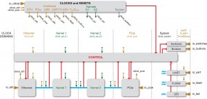
Figure 1 — A detailed hardware implementation of a two-function algorithm using traditional FPGA tools
The major roadblock to more-widespread FPGA adoption has been the complexity of implementing them. Until now, the only way to develop an application on an FPGA-based platform has been to deal with some of the lowest levels of hardware implementation. This has kept a large potential customer base—software developers—away from the devices and has made life increasingly complicated for traditional FPGA designers.
Recent methodologies for FPGA design, centered on high-level synthesis (HLS) tools and leveraging software programming languages such as OpenCL™, C and C++, have provided a sandbox for software developers to reap the benefits of FPGA-based hardware acceleration in numerous applications. But the methodologies often fall short in one essential respect: enabling software developers to define and configure, on their own, the hardware infrastructure best suited for their application. The industry has continued to pursue the holy grail of a high-level workflow for implementing applications on FPGA-based platforms that does not require specific FPGA expertise.
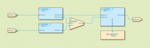
Figure 2 — A design example in QuickPlay
Over the past five years, PLDA has developed just such a workflow. Called QuickPlay, it efficiently addresses the implementation complexity challenge and enables multiple use models for FPGA development. But one of its core sources of value is the way in which it lets software developers take applications intended for CPUs and implement them, partially or fully, on FPGA hardware. QuickPlay leverages all of the FPGA resources, turning these powerful but complex devices into software-defined platforms that yield the benefits of FPGAs without the pain of hardware design.
Consider a software algorithm that can be broken down into two functions: Data is processed into one function and is then sent to another for further processing. From a software perspective, this implementation is as simple as a call to Function1() followed by a separate call to Function2(), using pointers to the location of the data to be processed.
Implementing such an algorithm on an FPGA-based hardware platform without the right hardware abstraction tool flow would require the software developer to come up with a hardware design resembling that in Figure 1 (where Kernel 1 and Kernel 2 are the respective hardware implementations of Function 1 and Function 2). The hardware design would need to include two elements: the control plane and the data plane.
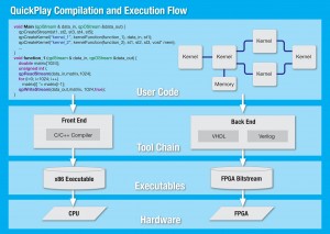
Figure 3 – QuickPlay features a straightforward design flow
The control plane is the execution engine that generates clocks and resets, manages system startup, orchestrates data plane operations, and performs all housekeeping functions. The data plane instantiates and connects the processing elements, Kernel 1 and Kernel 2, as well as the necessary I/O interfaces required to read data in and write processed data out. In our example, those interfaces are Ethernet and PCI Express (PCIe), as Figure 1 shows, though different application requirements will call for different I/O interfaces.
A software developer could easily generate Kernel 1and Kernel 2 using an HLS tool that compiles the software functions Function1() and Function2(), typically written in C or C++, into FPGA hardware descriptions in VHDL or Verilog, without requiring specific hardware expertise. Every other element in the design that is not algorithmic in nature (interfaces, control, clocks and resets), however, could not be generated with HLS tools, and hardware designers would have to design them as custom hardware description language functions or IP. The job of sourcing those elements and connecting them poses yet another challenge, as some elements may not be readily available or may have different interfaces (type and size), clocking requirements, specific startup sequences and so on.
Beyond the design work—and equally challenging—is the implementation work, which includes mapping the design onto the resources of the selected FPGA platform, generating the appropriate constraints, and confirming that those constraints are met after logic synthesis and implementation on the FPGA hardware. It can take even an experienced hardware designer weeks to achieve a working design on a new piece of FPGA hardware.
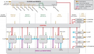
Figure 4 — The debug infrastructure is automatically created
Thus, any tool that aims to enable software developers to augment their applications with custom hardware must be able to:
- create functional hardware from pure software code;
- incorporate existing hardware IP blocks if needed;
- infer and create all of the support hardware (interfaces, control, clocks, etc.);
- support the use of commercial, off-the-shelf boards and custom platforms;
- ensure that the generated hardware is correct by construction so that it requires no hardware debug; and
- support debug of functional blocks using standard software debug tools only.
PLDA engineered QuickPlay from the ground up to meet all of those requirements, thereby enabling pure software developers to specify, build and integrate FPGAs into their software architectures with minimal effort.
SOFTWARE-CENTRIC METHODOLOGY
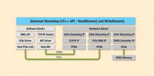
Figure 5 — Selecting the desired protocol sets up the required hardware and software stacks
The overall process of implementing a design using QuickPlay is straightforward:
- Develop a C/C++ functional model of the hardware engine.
- Verify the functional model with standard C/C++ debug tools.
- Specify the target FPGA platform and I/O interfaces (PCIe, Ethernet, DDR, QDR, etc.).
- Compile and build the hardware engine.
The process seems simple; but if it is to work seamlessly, it is critical that the generated hardware engine be guaranteed to function identically to the original software model. In other words, the functional model must be deterministic so that, no matter how fast the hardware implementation runs, both hardware and software executions will yield the exact same results.
Unfortunately, most parallel systems suffer from nondeterministic execution. Multithreaded software execution, for example, depends on the CPU, on the OS and on nonrelated processes running on the same host. Multiple runs of the same multithreaded program can have different behaviors. Such nondeterminism in hardware would be a nightmare, as it would require debugging the hardware engine itself, at the electrical waveform level, and thus would defeat the purpose of a tool aimed at abstracting hardware to software developers.
QuickPlay uses an intuitive dataflow model that mathematically guarantees deterministic execution, regardless of the execution engine. The model consists of concurrent functions, called kernels, communicating with streaming channels. It thus correlates well with how a software developer might sketch an application on a whiteboard. To guarantee deterministic behavior, the kernels must communicate with each other in a way that prevents data hazards, such as race conditions and deadlocks. This is achieved with streaming channels that are (1) FIFO-based, (2) blocking read and blocking write, and (3) point-to-point.
Those are the characteristics of a Kahn Process Network (KPN), the computation model on which PLDA built QuickPlay. Figure 2 shows a QuickPlay design example illustrating the KPN model.
The contents of any kernel can be arbitrary C/C++ code, third-party IP or even HDL code (for the hardware designers). QuickPlay then features a straightforward design flow (Figure 3).
Let’s take a closer look at each step of the QuickPlay design process.
Step 1: Pure software design. At this stage you create your FPGA design by adding and connecting processing kernels in C and by specifying the communication channels with your host software. QuickPlay’s Eclipse-based integrated development environment (IDE) provides a C/C++ library with a simple API to create kernels, streams, streaming ports and memory ports, and to read and write to and from streaming ports and memory ports.
In addition, the QuickPlay IDE provides an intuitive graphical editor that allows you to drag and drop kernels and other design elements and to draw streams.
Step 2: Functional verification. In this step, the focus is on making sure that the software model written in Step 1 works correctly. You do this by compiling the software model on the desktop, executing it with a test program that sends data to the inputs, and verifying the correctness of the outputs. The software model of the FPGA design is executed in parallel, with a distinct thread for each kernel to mimic the parallelism of the actual hardware implementation.
You would then debug your software model using standard software debug techniques and tools such as breakpoints, watchpoints, step-by-step execution and printf. (You will probably want to run more tests once the implementation is in hardware; we’ll deal with that shortly.) From a design flow standpoint, this is where you do all of your verification. Once you are done with this debug phase and have fixed all functional issues, you will not need any further debugging at the hardware level.
It’s important to remember that the functional model involves none of the hardware infrastructure elements. In the example above, the focus is on a simple, two-function model; none of the system aspects added in Figure 1 (such as the communication components, the control plane, and clocking and resets) are in play during this modeling and verification phase.
Step 3: Hardware generation. This step generates the FPGA hardware from your software model. It involves three simple actions:
- Using a drop-down menu in the QuickPlay GUI, select the FPGA hardware into which you want to implement your design. QuickPlay can implement designs on a growing selection of off-the-shelf boards that feature leading-edge Xilinx® All Programmable FPGAs, PCIe 3.0, 10-Gbit Ethernet, DDR3 SDRAM, QDR2+ SRAM and more.
- Select the physical interfaces (and therefore the protocols) to map to the design input and output ports. These are also simple menu selections. The choice will depend on the interfaces that are available on the FPGA board you have selected, such as PCIe, TCP/IP over 10-Gbit Ethernet and UDP over 10-Gbit Ethernet. Selecting the communication protocol automatically invokes not only the hardware IP block required to implement the connection, but also any software stacks layered over it, so that the complete system is created.
- Launch the build process. This will run the HLS engine (creating hardware from C code), create the needed system hardware functions (the control plane logic in our original example) and run any other tools necessary (for example, Xilinx’s Vivado® integrated design environment) to build the hardware images that the board will require. No manual intervention is required to complete this process.
Step 4: System execution. This is similar to the execution of the functional model in Step 2 (functional verification), except that now, while the host application still runs in software, the FPGA design runs on the selected FPGA board. This means that you can stream real data in and out of the FPGA board and thereby benefit from additional verification coverage of your function. Because this will run so much faster, and because you can use live data sources, you are likely to run many more tests at this stage than you could during functional verification.
Step 5: System debug. Because you’re running so many more tests now than you were doing during the functional verification phase, you’re likely to uncover functional bugs that weren’t uncovered in Step 2. So how do you debug now?
As already noted, you never have to debug at the hardware level, even if a bug is discovered after executing a function in hardware. Because QuickPlay guarantees functional equivalence between the software model and the hardware implementation, any bug in the hardware version has to exist in the software version as well. This is why you don’t need to debug in hardware; you can debug exclusively in the software domain.
Once you have identified the test sequence that failed in hardware, QuickPlay can capture the sequence of events at the input of the design that generated the faulty operation and replay it back into the software environment, where you can now do your debug and identify the source of the bug using the Eclipse debugger.
This is possible because QuickPlay automatically provisions hardware with infrastructure for observing all of the critical points of the design. You can disable this infrastructure to free up valuable hardware real estate. Figure 4 shows the example system with added debug circuitry. Without QuickPlay, some sort of debug infrastructure would have to be inserted and managed by hand; with QuickPlay, this all becomes automatic and transparent to the software developer.
The overall process is to model in software, then build the system and test in hardware. If there are any bugs, import the failing test sequences back into the software environment, debug there, fix the source code and then repeat the process. This represents a dramatic productivity improvement over traditional flows.
Step 6 (optional): System optimization. Once you have completed the debug phase, you have a functional design that operates on the FPGA board correctly. You may want to make some performance optimizations, however, and this is the proper time to do that, as you already know that your system is running correctly.
The first optimization you should consider is to refine your functional model. There are probably additional concurrency opportunities available; for example, you might try decomposing or refactoring functions in a different way. At this level, optimizations can yield spectacular performance improvements. Needless to say, doing so with a VHDL or Verilog design would require significant time, whereas doing the modifications in C would be a quick and straightforward process.
Second, you may want to try a different FPGA board with a faster FPGA. Because the mapping from the functional model to the board is so easy, it’s a simple matter to try a variety of boards in order to select the optimal one.
The third optimization has to do with the hardware kernels that QuickPlay creates via high-level synthesis. While the resulting hardware is guaranteed to operate correctly and efficiently, it may not operate as efficiently as hardware handcrafted by a hardware engineer. At this stage, you have several options: You can optimize your code and tune QuickPlay HLS settings to improve the generated hardware, use Vivado HLS to generate more-efficient hardware, or have a hardware designer handcraft the most critical blocks in HDL.
None of these optimization steps is mandatory, but they provide options when you need better-performing hardware and have limited hardware design resources available. A hardware engineer may be able to help with these optimizations. Once you have made any of these changes, simply repeat the build process.
A UNIVERSAL STREAMING CONDUIT
QuickPlay provides a universal streaming API that entirely abstracts away the underlying physical communication protocol. Streaming data is received via the ReadStream() function and is sent out using the WriteStream() function. Those functions can be used to send and receive data between kernels, to embedded or board-level memory, or to an embedded or external host CPU, thus providing broad architectural flexibility with no need for the developer to comprehend or manage the underlying low-level protocols.
The selected protocol determines the hardware through which that data arrives and departs. At present, QuickPlay supports ARM® AMBA® AXI4-Stream, DDR3, PCIe (with DMA) and TCP/IP; more protocols are being added and will be added as demand dictates. Selecting the desired protocol sets up not only the hardware needed to implement the protocol, but also the software stacks required to support the higher protocol layers, as shown in Figure 5.
QuickPlay manages the exact implementation of these reads and writes (size, alignment, marshaling, etc.). The most important characteristic of the ReadStream() and WriteStream() statements is that they are blocking: When either statement is encountered, execution will not pass to the next statement until all of the expected data has been read or written. This is important for realizing the determinism of the algorithm.
The “binding” between the generic ReadStream() and WriteStream() statements and the actual underlying protocol hardware occurs at runtime via the QuickPlay Library. This not only prevents the communication details from cluttering up the software program, but also provides modularity and portability. The communication protocol can easily be changed without requiring any changes to the actual kernel code or host software. The ReadStream() and WriteStream() statements will automatically bind to whichever protocol has been selected, with no effect on program semantics.
As a result of the abstraction that QuickPlay provides, the software algorithms remain pure, focusing solely on data manipulation in a manner that’s completely independent of the underlying communication details.
PRODUCTION-QUALITY OUTPUT
Depending on the HLS tool being used, results might be improved by learning coding styles that result in more efficient hardware generation, but that is optional.
While in other situations the hardware platform you use may be viewed simply as a prototyping vehicle, the systems you create using QuickPlay are production-worthy. Going from a purely software implementation to a hardware-assisted or hardware-only implementation traditionally takes months. QuickPlay reduces that time to days.
The QuickPlay methodology achieves the long-sought goal of allowing software engineers to create hardware implementations of all or portions of their application. By working in their familiar domain, software engineers can make use of custom hardware as needed, automatically generating hardware-augmented applications that operate more efficiently and can be production-ready months ahead of handcrafted designs.
