

GaN as a wide-bandgap compound semiconductor material is perfectly suited for power switching devices that operate at significantly higher frequencies without suffering from major losses. This is due to their drastically lower on-state resistance combined with considerably reduced in/output capacitances. Higher switching frequencies lead to a substantial volume reduction of passive components such as inductors, transformers and capacitors. Manufacturers of GaN-on-Si wafers such as EpiGaN are striving to make GaN wafer processing compatible with the tools and procedures in existing Si-CMOS fabs.
The future of power electronics has arrived: applications of GaN transistors, including battery chargers, motor drives, solar inverters and consumer-oriented power supplies, are gaining visibility. They all point to significant performance improvements. Most of the top-20 electronic device and system manufacturers have defined their strategies to leverage the advantages of wide-band-gap semiconductors for their next-generation products.

fig 1: EpiGaN epi-wafers
The very promising market outlook for commercial GaN products allows epi-wafer suppliers such as EpiGaN to think about standardization procedures for GaN-on-silicon wafers, as these are mandatory for improved product stability in high-volume manufacturing processes. EpiGaN offers wafer structures with defined targets in terms of their electrical characteristics, especially in their latest generation of wafers up to 200mm in diameter for 650V power switching devices. Manufacturing these wafers is not an easy task since stack structures have to be carefully controlled to meet the higher voltage requirements together with strict bow specifications as required by Si-CMOS manufacturing lines.
On the Road to 1.2 and 2 kV
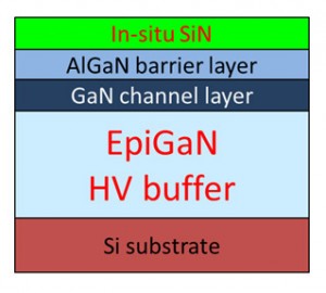
Fig 2: Layer structure
EpiGaN now manufactures GaN-on-silicon wafers with a breakdown voltage above 1000V and lateral leakage currents below 100nA/mm at the rated voltage of 650V. Yet this is by no means the upper limit. Recent research work has yielded FETs with a breakdown above 2kV. Today’s limitations in regard to breakdown voltage are confining GaN transistors to power electronics products in the 30 to 600V range.
However, devices with 600V breakdown voltage have been released recently by several chipmakers. It won’t take long before devices operating at 1,200V can be added to the list. This will enable the replacement of two silicon MOSFETs with a single GaN HEMT – a move that will substantially trim the cost and weight of power converters that operate at much higher switching frequencies compared to incumbent Si-based solutions.
Making Gallium-Nitride Devices Affordable
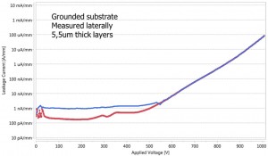
Fig 3: Latest generation: low leakage up to 650V
Wide-band-gap semiconductor AlGaN/GaN heterostructures belong to a superior class of materials. Their bandgap has a value of 3.4eV to 6.2eV, depending on the material composition. This large bandgap enables GaN devices to work at higher temperatures due to low intrinsic carrier concentrations. Because its field strength is an order of magnitude higher than that of silicon, and also due to high carrier mobility and concentration associated with the two-dimensional electron gas (2DEG) formation at the interface of an AlGaN/GaN heterostructure, such devices in switching applications offer a low on-resistance combined with low-loss high-frequency switching.
GaN-on-Silicon currently is the most cost-efficient wide-bandgap technology, and is well suited to benefit from the economies of scale of the established Si technology. GaN-on-Si has developed to a point where it is feasible to deposit advanced heterostructures on silicon wafers of up to 200mm in diameter. There is also an ongoing effort to develop process compatibility with standard Si-CMOS technology. This would open the door to further cost reductions by using the existing lines at 200mm silicon fabs.
GaN Replacing Si in Power Devices
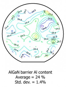
Fig 4: AlGaN Barrier Uniformity on 150mm substrates
In the ever-so-fast changing world of semiconductors, the industry strives to improve and innovate out of an inherent necessity. No doubt, Si power electronics is nearing its theoretical limits and only incremental performance improvements are still possible. . A recent study by French market researcher Yole Development foresees the annual market volume for GaN devices surpassing $300M in 2020. This involves a compound growth rate of 95 percent from today’s modest level of about $20m.
MOCVD reactors have been used for a long time to produce epitaxial wafers for lasers, LEDs and RF components. Growing GaN-on-Si is different, since there are some factors that need special attention. Of foremost concern is the mechanical stress occurring in GaN-on-Si wafers due to the severe crystalline and temperature mismatch between GaN and Silicon. Without sophisticated strain engineering in a sequence of buffer layers this incompatibility of basic material parameters would lead to intolerable wafer warping and cracking.
EpiGaN Uses In-situ SiN Passivation
EpiGaN is specifically engaged in developing a solution for sealing the top of their GaN-on-Si wafers directly after growth. This is done in the form of an in-situ grown Silicon-Nitride (SiN) passivation layer, which is about 50nm thick. As a consequence, there is no exposure of (Al,Ga)N to the fab environment. This circumstance will facilitate entrance of the GaN-on-Si technology into Si-CMOS fabs.
EpiGaN is a leader in pioneering this in-situ SiN surface passivation. The process was derived from the MOCVD growth of SiN using surface electrical passivation for III-Nitrides. EpiGaN applies this to much broader purposes, among them a unique gate dielectric with a smooth and contamination-free surface.
The in-situ SiN capping layer also controls the filling of the surface states during device operation. SiN can provide enough charge to neutralize the surface charge of the AlGaN barrier layer in a GaN-on-Si device so that its surface potential no longer contributes to 2DEG depletion. In addition, the SiN layer adds device stability at elevated temperatures.
Another benefit of the SiN cap layer is that it enables a higher aluminum concentration in the (Al,Ga)N barrier without significant material degradation. This is not the case in transistor structures with an uncapped or GaN-capped AlGaN/GaN quantum well, where the onset of relaxation of the strained top AlGaN layer prevents using a high aluminum content.
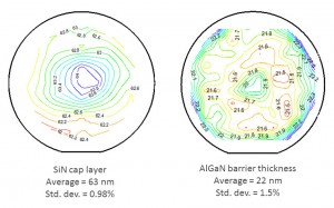
Fig 5: SiN Thickness Uniformity on 150mm substrates
In combination with the in-situ SiN deposition it is possible to replace the AlGaN layer with a pure AlN layer. For such an SiN/AlN/GaN layer design, sheet resistance falls below 250Ω/sq. Hall measurements indicate that the electron sheet concentration is larger than 2x 1013 cm-2 and electron mobility above 1,000 cm2/Vs. These values look very promising and they enable the fabrication of transistor devices with higher higher current densities. This feature could enable a smaller device – thus lower costs – for the same current rating.
Favorable Electrical Properties
Regarding economies of scale, GaN-on-Si devices show an advantage because they offer inherently better electrical properties than Si, specifically a much lower on-resistance in relation to the active area. Additionally, the conduction and switching losses are significantly lower for GaN compared to Si FETs. In other words, more power can be extracted in a more efficiently manner from a device of the same active area. Four or five times more current can be drawn from a GaN device than from a Si device of the same size
Heat dissipation follows the same inherent laws but it is of some practical concern. GaN can withstand much higher operating temperatures than Si junctions.. But heat dissipation from a much smaller active area becomes a problem to be dealt with in an appropriate manner. With higher power loads on smaller devices specific cooling measures must be taken. As a consequence, packaging technology has to catch up and support the superior performance of this new generation of devices.
System Lay-out Considerations
Higher switching frequencies will force power system designers to re-design the magnetics components involved, especially in PFC (power factor correction) applications. Switch-mode power supplies (SMPS) with PFC for consumer laptops using GaN devices are three to five times smaller in size, six times lighter in weight and they typically operate up to a few hundred MHz. This implies that system designers have to consider different passive component and packaging materials. Shielding and cooling structures as well have to be re-optimized for GaN.
GaN Epitaxy for Power Swtiching, RF and Sensor Electronics
EpiGaN, founded in 2010 as a spin-off from Belgian research center Imec, has become a key player in GaN-on-Si semiconductor wafer fabrication. The company is paving the way for replacing conventional silicon power semiconductors with GaN HEMTs (high-electron mobility transistor), thus enabling more efficient power supplies, motor drives, solar inverters and transportation systems. Since May 2012, EpiGaN is operating a volume wafer production facility at its headquarters on the Research Campus Hasselt in Belgium.
EpiGaN currently offers state-of-the-art GaN epitaxial layers deposited crack-free on Si-wafers for power switching and sensor applications or, for specific RF power applications, also on SiC. Foremost among EpiGan’s capabilities are the in-situ SiN capping layer for surface passivation and as a robust materials for enhanced device stability. Wafer diameters up to 200 mm are being offered with SiN/AlGaN/GaN, SiN/AlN/GaN and (Al/In/Ga)N/GaN based heterostructures.
These larger wafer sizes will spur a cost reduction and enable GaN to deliver in a field where until now no compound semiconductor has seriously challenged traditional silicon devices.
Author:
Dr. Markus Behet, Chief Marketing Officer at EpiGaN
Kempische Steenweg 293
B-3500 Hasselt – Belgium
