

Image capture of real-world scenes and blending this with virtual information represented as visual patterns is a vital tool in a growing number of industrial, medical and consumer applications. This new CMOS image sensor is used in a new imaging device for non-invasive cancer assessment. It forms the heart of a custom developed camera, which is used by FFOCT (Full Field Optical Coherence tomography) endoscopes for in-vivo optical probing as well as fast ex-vivo microscopy. The new CSI2100 sensor features an extremely high full-well capacity of 2 million electrons in its 1440×1400 pixels and a frame rate up to 500fps.
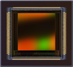
Fig 1
Advanced image-capture applications are opening up in a broad variety of products and systems. Yet there is no one specific image sensor to serve all those different conditions. Every system is best served with a specific imager optimized and designed to match the prevailing application and user requirements. (Figure 2) This is especially true for industrial and medical vision applications.
Thus, such digital camera applications require carefully laid-out image sensors adapted to deliver the best possible results in terms of resolution, noise, speed, spectral sensitivity, robustness, life cycle and price point. A comparison with natural vision capabilities in animals is helpful in this regard: birds of prey, snakes and cats all depend on very different kinds of visual input in terms of spectral sensitivity, field of view and resolution. As a consequence their “image sensors” have evolved to match the specific circumstances and necessities of their lives.
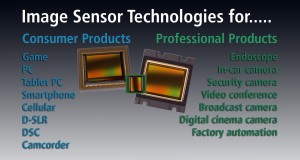
Fig 2
High Full-Well Capacity
A good example of sensor specialization is the new high-speed CMOS image sensor CSI2100 made by CMOSIS targeting demanding scientific and medical applications. With its global-shutter layout of 1440 x 1440 pixels at a pixel pitch of 12µm, the CSI2100 achieves the extremely high full-well charge of 2 Me per pixel – delivering unprecedented resolution and detail richness in its dedicated field of optical tomography. It enables in-vivo inspection of human tissue down to the cell level as well as fast ex-vivo microscopy. The CSI2100 wafers are fabricated by the wafer foundry Tower Jazz in Migdal Haemek, Israel.
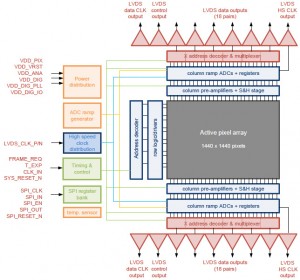
Fig 3
Besides its high full-well capacity the CSI2100 achieves high frame rates up to 500fps by integrating 35 LVDS (Low voltage Differential Signaling) outputs. Dark noise, mainly caused by ADC quantization noise, is held to 945e-. Dynamic range is 66dB. The chip, housed in a small µBGA package with 173 pins, has a power consumption of just 2 watts (Figure 3).
The new sensor was conceived within the EU-funded FFP7-ICT project “CAReIOCA” (Non-Invasive Optical Biopsy for Cancer Assessment Using Ultra-high Resolution Full-Field Optical Coherence Tomography) started in 2013. The program is continuing at a fast pace developing and evaluating high-resolution/high-speed medical imaging devices for performing non-invasive optical biopsy procedures by building volumetric images through a Linnik interferometer analysis of the interference patterns of light reflected by the examined tissue and a reference light source via an oscillating mirror. This way, living cells of 5µm in diameter can be captured and examined.
A major scientific goal of the CAReIOCA program is to establish atlases of specific FFOCT histology imagery for clinical use, foremost in the diagnostics and post-surgical evaluation of cancer. This part is carried out by Leiden University, The Netherlands, and Gustave Roussy Institute in Villejuif (Paris). Optical biopsy is meant to ease the burden on cancer patients by avoiding the destructive removal of tissue probes for traditional biopsy and histological analysis procedures.

Fig 4
By the end of 2014 CAReIOCA had progressed to demonstrating prototypes of a handheld FFOCT endoscope containing the compact 2-MP camera Q-2A750/CXP with CoaXPress interface, integrating the CMOSIS sensor CSI2100. This new diagnostic prototype system shows a 5 times higher processing speed and a 3 times higher sensitivity compared to existing designs.
CMOS Sensor Trends
CMOS sensors and cameras have developed to a point where they capture near-perfect imagery. Their advantage compared to the older CCD imagers is that they can be narrowly tailored to their specific application fields. In
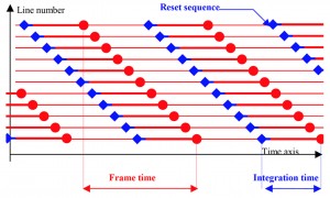
Fig 5a
addition, CMOS sensors, by virtue of their operational principle and established manufacturing processes as CMOS semiconductor devices, integrate on the same chip image capture with multiple support functions.
Such support functions include image processing for high dynamic range (HDR), on-chip noise suppression, flexible channel multiplexing, windowing and subsampling, and high-speed LVDS interfacing. All this leads to more compact camera designs, better system interconnect and compatibility, and ease of use.
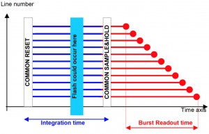
Fig 5b
High data throughput is very much in demand for industrial vision, especially in production and inspection tasks. Users want to get as much data off their imagers as possible, asking for the highest possible frame rate for their specific applications. Throughput rates have increased over the past few years from 30 to 60 to about 120 to 240 frames per second.
Thus, sensors and cameras must be able to accommodate higher frame rates. CMOS cameras have improved to a degree where they outperform traditional CCD-based imagers. An off-the-shelf 12-Megapixel digital image sensor from CMOSIS, the CMV12000 Series, delivers 300 fps at full resolution (10 bits per pixel). Other sensors of the same product family show similar data rates with different resolutions. Even higher frame rates are feasible in windowing or subsampling modes.
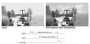
Fig 6
The same fast-paced progress of CMOS sensors applies to pixel count, or resolution. It has gone from 1.3 MP (SXGA) up to 2, 4, 8, 12 and 20 Megapixels. Higher resolution enables cameras to capture more details that can be analyzed within one image with a wide field of view (Figure 4). This is advantageous in traffic management applications, where one high-resolution camera can now track up to four lanes of traffic instead of having to deploy four individual lane cameras.
In the light of this technological progress, a resolution of 3.5 – 4K is standard today in traffic and video recording applications. For high-end industrial inspection, as in flat-panel inspection or aerial mapping, standard resolution is 20 MP. However this is not the end. The general trend points to still higher resolutions for global-shutter cameras. It might take another year to get up to 40 – 50 MP. This is where rolling-shutter sensors are still defending their turf: with pixel counts of up to 70 MP.
Demands on Image Capture Systems
- High sensitivity: This should be coupled with low noise levels as the foremost consideration of industrial users. High sensitivity will deliver enough image data at short exposure times. Low noise and high sensitivity also allow operation at a low light intensity by applying the proper gain if needed. High sensitivity across the visible spectrum should be accompanied by increased sensitivity in the near infrared.
- Low cost: Minimum system cost is best achieved via image sensor size reduction, optimization and if high-volume production for yield
optimization .
- High frame rate: This enables several shots of an object in a rapid-fire sequence to track and document its movements. This is supported by the technique of exposing one image while the previously taken image is being read out.
- High resolution: This equals a large field of view for delivering high image detail.
- No image correction: All these demands have to be implemented without impacting the raw image quality so that no extra off-chip correction is needed.
Global Shutter for CMOS Sensors
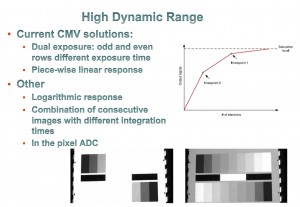
Fig 7
Combining a much smaller pixel layout with a global shutter is another major progress that imagers from CMOSIS have achieved in the last few years.
A global shutter exposes all pixels of a sensor at the same time and over the same duration. It is a more complex concept – and it was initially more costly to implement in CMOS sensors – because it requires some kind of a local storage element (usually a capacitor) inside each pixel, plus some control function to start and stop the exposure. All this enlarges pixel size.
A rolling shutter, in a marked difference, will expose an image sequentially, row by row, top to bottom, at different moments in time, much like the mechanical curtain rolling down behind the lens in an old-fashioned analog photo camera. This rolling effect causes time-related artifacts, which can skew the image of fast-moving objects as the exposure follows or deviates from their horizontal or vertical position at any given moment across the image plane (Figure 5). Another rolling shutter artifact occurs when illuminating the scene with a short-burst flash. The result is that only a few rows or parts of the image are exposed, whereas other areas remain dark.
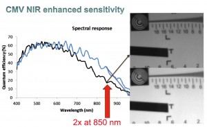
Fig 8
The rolling shutter concept has been the traditional method also in digital imaging since it is much easier to build a pixel architecture adapted to the row-by-row exposure scheme. Therefore CMOS sensors with four-transistor pixel architecture usually come with a rolling shutter. The lower number of pixel transistors and state-of-the art layout results in pixels with excellent specs in regard of dynamic range and dark current. CMOSIS has developed high-end sensors for the M camera model of Leica Camera based on these rolling shutter pixels.
Providing a global shutter in a CMOS sensor is more complicated since it involves placing the storage capacity inside each pixel. This takes up space and leads to a larger pixel layout, which is more expensive.
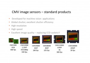
Fig 9
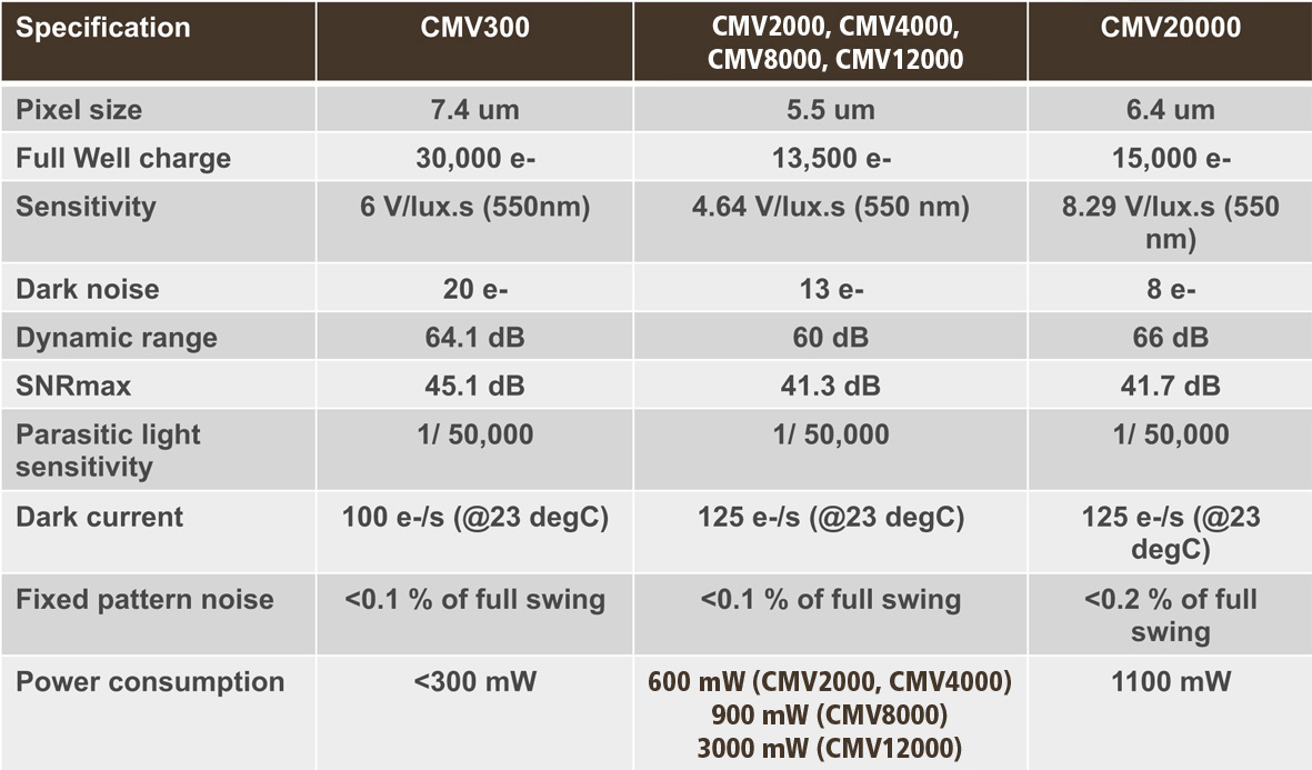
However, global-shutter technology as offered by CMOSIS has greatly improved. This primarily pertains to the capacitive storage nodes needed inside each pixel to hold the pixel values for reading them out sequentially after the exposure stops. Smaller storage nodes are now feasible with reasonably small pixel sizes and at lower price points. Advanced global-shutter CMOS sensor designs feature pixels down to 5.5 x 5.5 µm² as available in the CMOSIS CMV product family. The goal is having 3.6-µm pixels with a low noise global shutter in the near future.
Of course, this scaled-down CMOS layout requires fabs or foundries with wafer-processing capabilities that can accommodate these small pixel dimensions. It also needs comprehensive design know-how to create the appropriate pixel architecture and technology.
Eight-transistor Pixel Architecture
Fitting a low-noise global shutter to a CMOS image sensor requires a complex pixel architecture. But a specific new architecture is set to overcome this obstacle. The eight-transistor (8T) global-shutter architecture patented by CMOSIS differentiates it from the traditional 4T rolling shutter or the 5T global shutter concept. This eight-transistor pixel design is now implemented in all global-shutter sensor types of the CMOSIS CMV Series sensor family.
The crucial point is that the 8T architecture provides two storage elements inside the pixel, rather than just one (as in the 5T structure). They separately store an image taken at the beginning of the exposure, and another one at the end of the exposure period. Deploying a clever algorithm, both these images are subtracted during readout to lower the total noise account and increase the shutter efficiency.
This way, noise levels below 10 electrons can be reached, and a shutter efficiency of 99.999 percent has been demonstrated. The technique, called correlated double sampling (CDS), enables the lowest fixed-pattern noise and low parasitic-light sensitivity when compared to 5T layouts or other designs.
Time-Delayed Integration
Time-delayed integration (TDI) imaging is another clever way to better capture moving objects. By synchronizing pixel exposure with the motion of the camera or the object, the effective exposure time can be increased. TDI implementation in CMOS has traditionally been difficult because of the lack of a charge-addition circuit. The application requires the combination of a global shutter and a low-noise readout method. Recently TDI in the digital domain, enabled by high frame rates, has become more and more popular, even though the improvement signal-to noise ratio improvement is lower than for the traditional TDI operation.
High Dynamic Range (HDR)
Another factor in improving global-shutter CMOS sensors is applying a specific method to achieve a high dynamic range (HDR). HDR expands the scale of the captured light and dark areas of an image to depict them in a satisfactory way. This is appropriate when capturing an image before a bright sky background or against very bright light sources, which tends to deliver overexposed images with blurred-out white areas, whereas the darkest shadows appear underexposed and recede into an unstructured black. Thus, the exposure levels for both light and dark areas have to be equalized across the image.
The reason for the unbalanced treatment of light and dark areas is the linear response curve of CMOS image sensors as opposed to the exponential, or logarithmic, behavior of the human eye. HDR is helpful in traffic applications for subduing glaring reflections when reading license plates or countering the over exposure effects of bright headlights.
The desired logarithmic response in a CMOS sensor can be achieved on-chip in several different ways:
- by sequential image capture using widely varying exposure times, thereby recording the light and dark areas separately,
- by equipping the sensor’s odd and even rows with different sensitivities for light and dark and calculating an appropriate average value for all regions of the image (Figure 6), or
- by using a piece-wise linear response (PLR), which delivers a more logarithmic ramping of the sensor’s response curve (Figure 7).
The user can choose the best suited method depending on the application, as they all have their specific benefits and drawbacks.
Enhanced NIR Sensitivity
Extending the spectral range of CMOS sensors to the near-infrared realm is becoming more and more important as a market trend (Figure 8). This especially applies to traffic applications but also to machine vision, because it allows the illumination of the scene to be monitored with flash lights that are invisible to the human eye.
About CMOSIS
CMOSIS, the leading European supplier of advanced CMOS image sensor solutions, is a pure-play supplier of standard off-the-shelf and application-specific CMOS image sensors for the industrial and professional market covering applications such as machine vision, scientific, medical, automatic data capture and space. CMOSIS is a fabless CMOS image sensor vendor providing in-house design, characterization and qualification facilities for research, development and volume production. CMOSIS currently employs more than 100 people in locations in Antwerp (Belgium), Funchal (Portugal), Nuremberg (Germany) and Cary (NC, USA).
The CMOSIS technology portfolio is based upon crucial IP related to various advanced aspects of line, area and endoscopic CMOS image sensors – among them high pixel counts at a high fill factor, high-speed functionality, large bit-depth of column ADCs, high dynamic range, TDI (time-delay and integration) implementation in CMOS and novel rad-hard pixel concepts.
Author
Pieter Willems is Manager Standard Products at CMOSIS in Antwerp, Belgium.
