
Forty years back when I got my first watch, I had to wind it up to fuel the mechanical spring to keep it going. Not many years after, digital watches got introduced, that ran from a small coin cell battery that had enough energy to keep it running for at least one year. Nowadays, we are loading our wearable wrist worn device (since you cannot call it just a watch anymore) with lots of sensors to make it a smart system. The watch is becoming an interface between the human body and the smart phone, enabling you to retrieve vital-and environmental-parameters to monitor your daily health and to measure your activity and exercise performance. It can measure parameters like heart rate, body-temperature, movement & activity, oxygen saturation and much more. All this recorded data finally can be uploaded into the cloud to be analyzed afterwards and to enable you to adapt your behavior where needed. When adding more sensors however, the battery life of the device is reducing, accordingly. Since we don’t want to increase size to allow bigger batteries, or charge our device more frequently, sensor companies started to develop more efficient smart sensors and sensor front-ends. These sensor devices reduce the overall power consumption without degrading the performance of the measured parameters.
Analog Devices (ADI) has developed sensors and senor front-ends to address all of the issues mentioned above. In this article you will learn more about the ADPD103 photometric front-end IC, its performance, its feature set and why this device has been developed for this new emerging wearable health monitor market.
Heart-rate monitoring goes hand in hand with analyzing the performance of your cardiac system. For that reason, heart rate is one of the most important parameters to monitor. We are
not just interested in the number of beats per minute, as a significant amount of information can be obtained as well from heart rhythm and heart rate variation [HRV]. Depending on the level of activity, the rhythm should be more or less a constant parameter, however with a slight variation. Very little heart rate variation can be translated into emotional arousal or stress. This is a parameter used for instance during sleep studies. A fast-changing heart-rhythm is not good either, as this could be an indicator of a cardiac disease like atrial fibrillation.
Monitoring heart rate and heart activity is classically being performed by bio-potential measurement. Electrodes are connected to the body, for example in a chest strap, to measure electrical activity in the cardiac tissue. Since this measurement principle requires an electrical connection at each side of the heart, it is difficult to integrate in wrist worn devices.
A single-point measurement for heart-rate, to be integrated in a wrist worn device, can be achieved by an optical measurement principle, called Photoplethysmography (PPG). This technology injects light into the surface of the tissue whereupon it is absorbed by the red blood cells and reflected back up to the tissue surface where it is measured with a photo
sensor. During the time of a heart-beat, the flow and volume of blood is changing, resulting in scattering of the amount of light. The heart-rate is a function of the reflected light, as seen by the photo sensor.
Mechanical Design Trade-offs
While designing an Optical Heart-rate monitor there are various aspect which should be carefully considered. Optically, we can measure by transmission or reflection. Transmitting light through a certain part of the body and receiving it at the opposite side, is best. The finger for instance is a very good location, where light can be sent from one side, and measured on the other side. Signal strengths for transmission measurement are roughly 30dB better than what is available in a measurement principle using a reflection technology. However, since transmission measurement is usually hard to integrate from mechanical standpoint, reflective measurement is a more common principle. For reflective measurement in a body worn device, the wrist is the most obvious location to measure, but also the most challenging one. Bone at the upper side of the wrist with limited arteries and capillaries and so pulsatile blood-flow make it difficult to get a decent receive signal. In general, for wrist worn devices, where arteries are not located on top of the wrist, you need to pick up pulsatile components from capillaries just under the surface of the tissue. For this use-case, green light at a wave-length between 500-550nm is most effective, as it doesn’t penetrate very deeply into the tissue and is highly absorbed by hemoglobin leading to a large signal with pulsating blood volume. By measuring at a location with solid blood flow, such as upper arm, temple or earlobe, the receive signals are usually much better. Red or Infra-Red light sources are suggested in this situation as they penetrate deeper into the tissue and provide the best reading by probing a large volume of blood.
Next to the importance of the chosen Transmit wave length, the position of the light source in relation to the photo sensor is an important aspect. With placing the LEDs too near at the photo sensor, the light doesn’t get the chance to travel through the tissue enough to get the right level of absorption. Also light reaching the photo sensor without penetrating the tissue at all, might result in saturation of the input stage. This could be the case by having a protection window between sensor and tissue. This phenomena is often referred to as; Internal Light Pollution (ILP), resulting in a DC offset and a poor AC modulation. Placing the LEDs too far from the photo sensor results in a weak receive signal, since the decay of light is exponential to the distance. Also from power point of view this is not optimal, as the level of the receive signal will be small in relation to the amount of power spent.
ADPD103 as an Electronic Signal Chain
After choosing and designing the optics in your system, the next step is making the electronic connection to the digital-world. The transmit- and receive-signal-chain can be designed discretely, however most wearable devices suffer from size constraints. When size isn’t the biggest obstacle though, it is better to invest in a bigger battery to extend battery life, rather than spending valuable board space on the electronics.
Analog Devices’ ADP103 provides everything needed in a high performance optical signal chain. It is a highly efficient analog photometric front-end with built in analog-to-digital converter (ADC) and I2C interface, designed for power- and size-critical applications, such as wearable electronics. Figure 1 shows the block-diagram of the device.
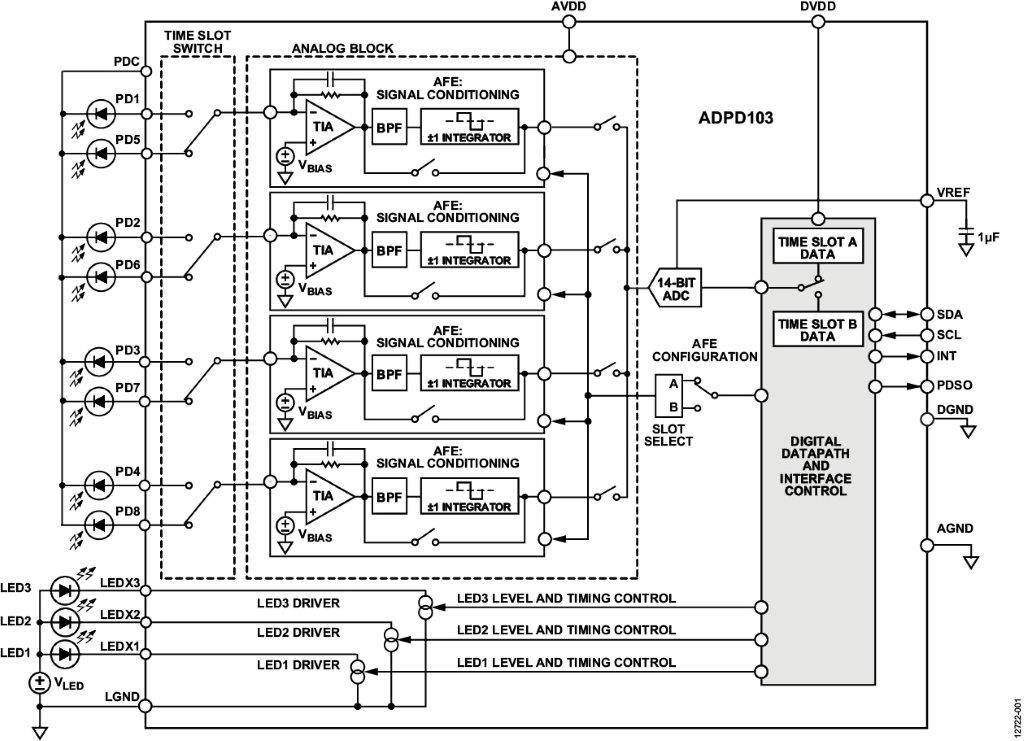
Fig. 1. ADPD103 Block Diagram.
When describing an electronic system, one usually starts with the sensor and input signal chain. However in an optical system, light reflection or absorption cannot be measured before a light pulse has been generated. Therefore we are starting with the ADPD103 transmit path, which supports three programmable LED-drivers that can operate in two independent time slots. Each of these time slots is carried out sequentially. The current sources are pulse-programmable and able to sink currents between 10 mA and 250 mA. In addition to magnitude, the pulse width and number of pulses are programmable by the integrated state machine of the ADPD103. Depending on the LED type and wavelength, there is flexibility to adjust the LED forward voltage. Since most of the portable systems are operating from a single coin cell battery, boost converters might be needed to increase the voltage above the battery supply voltage. The ADP2503/4 e.g. is able to fulfill these requirements.
At the receiver side, the ADPD103 has four identical input signal chains able to connect up to eight photo diodes. For each two photo diode inputs, a multiplexer is integrated, followed by a trans-impedance amplifier that converts the photo current into a voltage. The output of the amplifier is followed by a band pass filter and finally an integrator for synchronous demodulation. Besides amplification of the photo current, rejecting the ambient light interferes is the main objective of the analog signal chain. Sunlight isn’t the hardest interferer to block, however light sources such as fluorescent and energy-savings-lamps are hard to reject, as these can be seen as the signal of interest. The ADPD103 suppresses these interferes very nicely. To keep the flexibility, there is also a TIA-ADC mode, where the band-pass filter and integrator can be bypassed. Selection of which and how many photo sensor to use, depends on the overall use-case.
Most application require just one photo detector. For this scenario we recommend connecting the sensor to either input PD1 or PD5 to maximize the signal-to-noise performance. For maximizing the dynamic range, we recommend connecting the photo sensor to either the first four inputs or the last four inputs as shown in figure 2. It is also possible to connect multiple photo-diodes to your system either to increase sensitivity or to make it less sensitive to relative position on the body. Blockers in the receive signal chain like hairs or pigment spots can influence the overall performance drastically. Having access to multiple photo sensors gives more flexibility by being able to switch among the channels and select the input with the most optimal receive signal. Another option is to use multiple photo
sensors and use this as an optical proximity sensor. When the device is not worn on the body, all inputs roughly see the same optical input level. When having the device worn on the body however, the photo sensor closest to the excitation light source (LED) will see the highest signal level. This technology allows you to switch off the LEDs when the devices is not attached to the body which extends battery life.
Figure 3 visualizes the sequence of the transmit– receive-process inside the ADPD103. This view shows the timing for just one time slot.
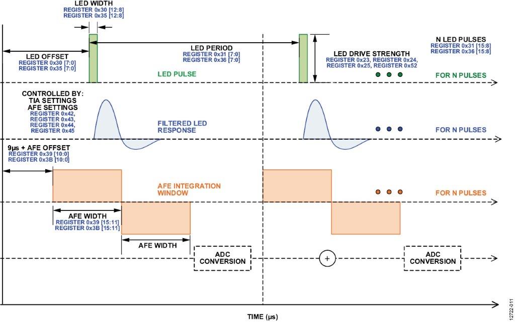
Fig 3. ADPD103 Operational Diagram of N Pulses, at One Time Slot.
After generating a LED pulse which can be programmed in amplitude and time, the photo current is measured and filtered by the transimpedance amplifier and integrated over a certain time window. The conditioned output of each of the integrators can be multiplexed into the 14-bit successive approximation register (SAR) ADC. The SAR ADC converts the signal of the photodiode output after every LED pulse into the digital domain at a sampling frequency which is programmable between 0.1 Hz to 2.6 kHz maximum. Each subsequent conversion result can be summed with the previous result (up to 255 pulses) to achieve a final maximum range of 20-bits for each sampling period. In figure 4, an example is shown of a measured PPG signal, sampled at a data rate of 10 Hz, using 5 pulses per sample.
Additional resolution can be obtained by accumulation and averaging the 20-bit result to get a maximum resolution of 27-bits. These results can be stored in a 32-bit register, however it is also possible to provide these results as just a 16-bit number. The reading can be accessed directly, or through the built-in FIFO. The features mentioned make the ADPD103 very flexible and applicable to a wide range of use cases.
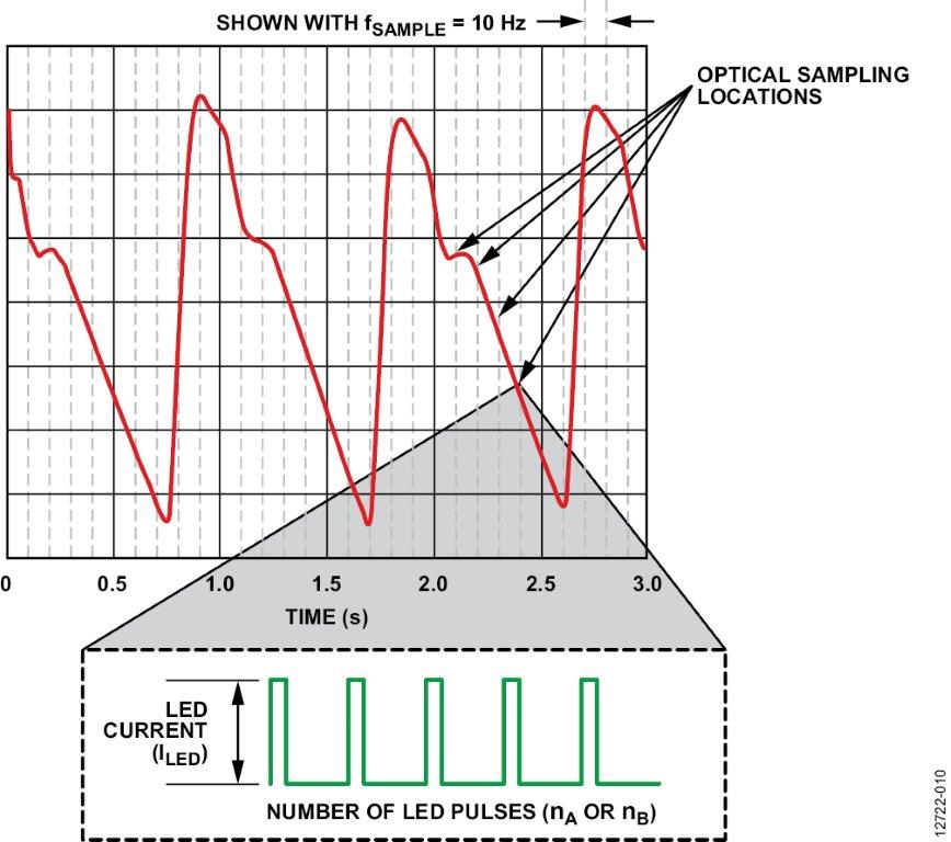
Fig 4. Sampled PPG Signal with Five LED Pulses per Data Point.
Optimizing SNR per WATT
While designing a sports watch, good performance at the lowest power dissipation possible, is the biggest challenge. The ADPD103 offers a variety of parameters which can be used to optimize the ratio between signal to noise and the amount of power spent. In several steps we are able to tune the system to find its operating “sweet spot.” With no photo current, the output of the ADC is at midscale. Therefore for maximization of the dynamic range, an offset can be applied to get an ADC code equal to zero, with no light at the input of the photo sensor. The following step is to set the normal operating point at approximately 60%, as this will leave enough headroom for detecting a heart-beat. To find this operating point we can tune the gain of the transimpedance amplifier in combination with
setting the maximum LED peak current. After optimizing the LED current and TIA gain, we can increase the number of LED pulses to get more signal. Be aware that increasing the LED peak current is increasing the SNR proportionally, whereas increasing the number of pulses by a factor of n, results in an SNR improvement of √(n) only.
Finding the optimum settings for your heart-rate device, also depends heavily on the user. The user’s skin tone has impact on the signal strength as well as device positioning, temperature and blood flow.
For calculating the power consumption, the optical front-end can be seen as two separate in power contributors:
Itotal = IADPD + ILEDs
IADPD is the current consumed by the input amplifier stage, the ADC and the digital state machine. These power numbers very much depend on the ADC sampling rate. The LED current, depends very much on the person’s skin tone and the position of the sensor on the body. For darker skin-tone more LED current is needed as well as for sensor position on the body with very little blood-flow. The average LED-current can be calculated with following equation:
ILED-average =
(ILED-PEAK x tpulse x npulses x Fsampling)
Ipeak is the max LED current, multiplied by the pulse width and the number of pulses. This can be seen as one timeslot and repeats every time a new sample is taken.
For a good Heart rate measurement on the wrist, a LED peak current is required around 125mA, using 2 pulses with 1us width per pulse. Considering a 100Hz sample frequency, the average LED drive takes 25uA.When we add 250uA average AFE current, the Optical front-end is consuming 275uA (@ 3V = 825uW ). In addition, we need to add the processor power as well as the power spent in the motion sensor. Especially for wearable devices, Analog Devices is providing extremely low power motion sensors, consuming just a few micro-amps for 3-axis measurement. The biggest power consumer in the system is the radio, where overall power consumption is very dependent on how often results will be uploaded to the host.
An auto-adaptive algorithm can help to improve the overall performance and power-consumption of your system. Each time the device is being used, small changes in the settings can be made to reach finally the optimum SNR performance and so HRM-accuracy, for the amount of power spent.
Sensitivity to Motion
Optical-based sport watches have a hard time coping with motion artifacts. Motion between the optical sensors (photo receiver and LED) and the skin, will influence the reading of the optical signal, since the measured signal will be a component of the reflected light in relation to the optical change coming from the motion. MEMs motion sensors can be used to measure the physical movement of the device and compensate the errors generated in the optical measurement. The ADXL362 is the product of choice for battery-powered and wearable products. This is a complete 3-axis MEMs motion sensor (Micro-Electro-Mechanical), measuring g-forces at mg resolution, and converting this directly into a digital value via its on-board 12 bit ADC. Depending of the selected output data rate, this sensor operates at 300nA up to 3.0uA, for a full 3-axis measurement at 400 Hz output data rate (ODR). For a proper working heart rate measurement system, the raw optical- and motion-data must be processed to yield the heart rate results that we’re ultimately interested in.
Other Use-cases for the ADPD103
This article has been focused on using the ADPD103 for optical heart rate systems, however, there are many other applications and use-cases where the ADPD103 can add value. In the medical market, blood oxygen (SPO2) is one of the other frequently used applications as well as non- invasive blood pressure, where PPG is one of the enabling measurements. Other markets where the ADPD103 has application are in lab equipment, gas sensors and industrial monitoring systems. For any application where a light source needs to be controlled and photo current needs to be measured, the ADPD103 can be the heart of your system, with, or without, a beat.