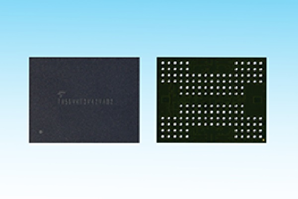
Toshiba Memory Corporation, the world leader in memory solutions, today announced development of the world’s first[1] BiCS FLASH™ three-dimensional (3D) flash memory[2] utilizing Through Silicon Via (TSV)[3] technology with 3-bit-per-cell (triple-level cell, TLC) technology. Shipments of prototypes for development purposes started in June, and product samples are scheduled for release in the second half of 2017. The prototype of this groundbreaking device will be showcased at the 2017 Flash Memory Summit in Santa Clara, California, United States, from August 7-10.
Devices fabricated with TSV technology have vertical electrodes and vias that pass through silicon dies to provide connections, an architecture that realizes high speed data input and output while reducing power consumption. Real-world performance has been proven previously, with the introduction of Toshiba’s 2D NAND Flash memory[4].
Combining a 48-layer 3D flash process and TSV technology has allowed Toshiba Memory Corporation to successfully increase product programming bandwidth while achieving low power consumption. The power efficiency[5] of a single package is approximately twice[6]that of the same generation BiCS FLASH™ memory fabricated with wire-bonding technology. TSV BiCS FLASH™ also enables a 1-terabyte (TB) device with a 16-die stacked architecture in a single package.
Toshiba Memory Corporation will commercialize BiCS FLASH™ with TSV technology to provide an ideal solution in respect for storage applications requiring low latency, high bandwidth and high IOPS[7]/Watt, including high-end enterprise SSDs.
General Specifications (Prototype)
| Package Type | NAND Dual x8 BGA-152 | ||
|---|---|---|---|
| Storage Capacity | 512 GB | 1 TB | |
| Number of Stacks | 8 | 16 | |
| External Dimension | W | 14 mm | 14 mm |
| D | 18 mm | 18 mm | |
| H | 1.35 mm | 1.85 mm | |
| Interface | Toggle DDR | ||
| Interface Max. Speed | 1066Mbps | ||
- Note:
- [1] Source: Toshiba Memory Corporation, as of July 11, 2017.
- [2] A structure stacking Flash memory cells vertically on a silicon substrate to realize significant density improvements over planar NAND Flash memory, where cells are formed on the silicon substrate.
- [3] Through Silicon Via: the technology which has vertical electrodes and vias to pass through the silicon dies for connection in a single package.
- [4] “Toshiba Develops World’s First 16-die Stacked NAND Flash Memory with TSV Technology”
https://toshiba.semicon-storage.com/ap-en/company/news/news-topics/2015/08/memory-20150806-1.html - [5] The rate of data transfer rate per power unit. (MB/s/W)
- [6] Compared with Toshiba Memory Corporation’s current products.
- [7] Input Output per Second: The number of data inputs and outputs for processing through an I/O port per second. A higher value represents better performance.