

NanoStreeM to assess the risks of nanomaterials in semiconductor manufacturing
On January 28, 2016, the 14 partners of the European NanoStreeM project gathered at imec for the project’s kick-off meeting. Together, they will build an inventory of all the nanomaterials that are used in today’s and future semiconductor manufacturing processes. The consortium will evaluate methodologies for risk assessment to protect human health and the environment. Imec’s Dimiter Prodanov, coordinator of the NanoStreeM project, talks about nanomaterials in semiconductor manufacturing and the precautionary approach to risk assessment and risk management.
Nanomaterials in the semiconductor fab
As Moore’s Law proceeds and transistor dimensions continue to shrink, a variety of novel nanostructured materials enter the semiconductor fab. Most of these materials have poorly understood hazardous properties. And this has become a shared concern of the semiconductor industry. Dimiter Prodanov: “Understanding how these materials affect human health, other biological systems and the environment is a relatively new area of scientific study. 50 how can we safely handle these materials? Which nanomaterials are being used and will be used in the future, and what is their potential danger? What is the risk for exposure by the fab workers? And how can the risks be assessed and managed? That will be the focus area of the Nano5treeM project. “The project, coordinated by imec, gathers 14 partners from 3 different worlds (R&D, industry and academia), active in various aspects of materials and semiconductor research and processing industry and academia), active in various aspects of materials and semiconductor research and processing.

Fig 1: Nanoparticles in solution
To be clear, the project will not deal with the risks of nanomaterials in consumer products. Dimiter Prodanov: “In fact, there are two approaches to nanotechnology. One is the bottom-up approach, where researchers or industry synthetize nanoparticles with special properties and introduce them in consumer products such as bicycles, paints, coatings, medicines or cosmetics. This will not be the focus of the project. NanoStreeM will deal with a second approach, the top-down approach to nanotechnology, where bulk materials are further processed to create nanoscale entities. In this approach, all the nanoscale objects are contained within packages, and nanomaterials are only used or released during certain steps of the processing. There is no concern for consumer exposure. But the fab worker can be exposed to nanomaterials during e.g. the maintenance of his equipment, or nanomaterials can be released into the environment.”
Identifying the hotspots of risk
The project builds on the earlier activities of a working group that was part of the ESIA community, the European Semiconductor Industry Association. This working group consisted of representatives from imec, STMicroelectronics, CEA, Fraunhofer and Intel. Its focus was on establishing best practices for CMP processing. CMP or chemical mechanical polishing uses nanoparticle abrasives for polishing, leading to waste slurries that can enter the environment. The use of nanomaterials in CMP slurries is now well documented, but there are other scenarios where nanomaterials may be used or generated. Dimiter Prodanov: “For example, different types of carbon-containing materials, such as graphene and carbon-nanotubes, start to enter the fab. There is growing evidence that unbounded carbon nanotubes -in the form of nanoparticles are health hazards. Experimental studies have pointed out that carbon nanotubes, when inhaled, can lead to sustained inflammation. In a semiconductor fab where nanoparticles are handled in containment, exposure to unbounded carbon nanotubes is not very likely. But there are situations where some exposure in not
unthinkable, such as the opening of a deposition reactor during maintenance. Part of the project’s mission will therefore be to map the trajectory of the various nanomaterials within a typical European facility and identify the hotspots of risk, where worker exposure is possible.”
Precautionary principle
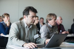
Fig 2: (Middle, left) Dimiter Prodanov, project coordinator, and (middle, right) Alain Pardon, Safety, Environmental & Health Manager atimec, at the kick-off meeting of the NanoStreeM project on January 28, 2016, at imec.
As the eco-and human toxicological properties of most of the engineered nanomaterials are largely unknown to the sector, most of the semiconductor fabs adopt the precautionary principle. Dimiter Prodanov: “As long as we don’t completely understand what is going on, we apply the precautionary principle when handling these materials: we assume that an unknown material has certain hazardous properties, and we take all the necessary precautions for handling this material safely. Later on, when there will be more experience and more scientific information on the material’s properties, we can lower the precautions or make them more focused.”
The properties of nanomaterials cannot simply be derived from their bulk counterparts. Dimiter Prodanov: “Materials at the nanoscale behave different from bulk materials due to quantum physics phenomena. Nanoparticles have a very large surface area compared to bulk material with an identical mass. And this increases significantly their catalytic activities. Also, the charge and surface energy distributions can be different. And this may change their chemical reactivity and lead to toxicological properties. For example, some materials can catalyze the formation of reactive oxygen species, which are pro-inflammatory in the body.”
Risk-banding tools
The precautionary principle is implemented by the use of so-called risk-banding tools, an approach that is also being followed at imec. Dimiter Prodanov: “At imec, the approach starts with grouping different nanomaterials into categories. We have 3 categories of supposed increasing hazard, and we have 3 categories of increasing likely hood of exposure. That makes a matrix of 9 categories, and all steps in a process can be categorized in this way. For each of the categories, we prescribe different safety measures. For example, when we know that there is a nanomaterial, but exposure is unlikely, the measure can be limited to post signing and labeling.
For another category, we will prescribe the use of directed ventilation, or , when needed, the use of a full breathing apparatus.
As part of the NanoStreeM project, we will compare the various risk banding approaches that are being used within the industry. We will share best practices and make recommendations for improvement.” Imec, besides coordinating the project, will share experience in this risk assessment, and will participate in the mapping exercise for future materials.
Outcome of the project
The European Union has taken concerted efforts to understand and promote nanotechnology, but also to address public concerns. Dimiter Prodanov: “With this Horizon 2020 project, we answered a call which was opened last year for support action in the area of ICT, and which aims
to look into the use and characterization of nanomaterials. By comparing various approaches to risk assessment and sharing good practices, the NanoStreeM project will contribute to improve the awareness and safety of the workers in semiconductor fabs, and minimize the impact on the environment. We will come up with recommendations concerning the use of nanomaterials in semiconductor processing. We will also set up comprehensive training and communication efforts.” But the project will also enable the semiconductor industry to share and benchmark its
approach with other sectors that face similar challenges, such as the pharmaceutical industry, the paint industry etc. Dimiter Prodanov: “The semiconductor industry is an advanced industry that is well aware of its duties and responsibilities. We have a very safety aware culture, resulting in a very tight process control. And this is an attitude that can be transferred to other industries as well. “
The NanoStreeM project (Nanomaterials: strategies for safety assessments in advanced integrated circuits manufacturing) receives funding from the European Union’s Horizon 2020 Research and Innovation Programme under grant agreement n° 688794.
Imec collaborates in many projects (EU, ESA and IWT) on which we work in close collaboration with industrial and academic partners. On our website, you can view the projects that are currently running. You can browse this information by research domain. And on April 30, 2076,
imec participates in Europe Day (Dutch website), where we will put some of our European projects in the spotlight.


