In short:
The team of Milos Nesladek from IMO-IMOMEC, an imec research group at University of Hasselt, has a long track-record of using artificial diamonds in the race to develop the best solid-state quantum system. In research that was recently published in Nature Communications they now demonstrate a viable approach for a quantum technology platform that operates at room-temperature via electrically-read electron-nuclear spin gates on a diamond electronic chip. This proof of concept is a first step towards more complex, electrically-read gates for advanced quantum technologies that can benefit from the long nuclear spin coherence in diamond.
Nuclear and electron spins in diamond quantum systems
Semiconductor spin qubit systems are promising candidates for future quantum technologies, such as quantum computing, telecommunication and sensing because of their potential for wide electronic scalability and nanoscale device integration. Nuclear spins in diamonds are particularly interesting because of their large coherence times which is important for performance and reliability of complex quantum applications. At ambient temperatures the coherence time is in the range of seconds; when cooled down to around 10K it even increases to tens of minutes.
Milos Nesladek: “Key to quantum applications for diamond is the nitrogen-vacancy (NV) center, a defect in the crystal where a nitrogen atom replaces one of the carbons adjacent to a free lattice space (a vacancy). The negatively charged NV center is one of the most attractive solid-state qubit platforms as it benefits from an electronic spin that can be used as a qubit or as an auxiliary qubit for reading dark nuclear spins. Having access to both the electron and the (nitrogen) nuclear spins offers many advantages as they fulfill different functions. Electron spins have shorter coherence times but offer a fast control, while more stable nuclear spins could be used, for example, as a memory qubit to store spin information from the electronic qubit.
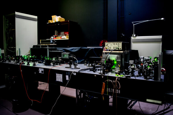
The optical table with a room temperature quantum microscope setup used in the single nuclear spin readout experiment.
The two types of qubits can also be entangled. Entanglement is an essential quantum process enabling quantum computers, it cuts down the information transfer time between qubits and is ultimately necessary for many other quantum applications such as quantum communication. So far, devices using quantum entanglement work mainly at ultra-low temperatures, close to absolute 0K.
Electrical readout at room temperature
Currently, the entanglement of a nuclear and electron spin is read out optically with bulky setups. Milos Nesladek: “We are interested in reading the spins states electrically, because it would open access to miniaturization and integration of electronic devices with several entangled modular electron-nuclear spin units on a single electronic quantum chip. These units can communicate in two ways. Firstly, one can place them close to each other, typically at less than 50nm, but then they cannot be resolved optically due to the diffraction-limit of optics. This poses a problem for operating the units individually and for using entangling quantum gates. To circumvent this, we fabricated electrical contacts around the NV centers in the units, which allows the units to be read individually.”
“With an electrical readout, the spatial resolution is solely determined by the electrode size which opens the way to placing spin-qubits in close proximity and ultimately to fabricate nanoscale quantum systems with semiconductor scalability. It has been successfully used to measure the spin state of large ensembles of nuclear spins recently, but fundamental quantum operations rely on the driving and readout of single qubits. Here, we show the electrical readout of a single nuclear spin of the NV center, mediated by a single electron spin,” says Milos Nesladek.
“Moreover, we demonstrate this at room temperature. One of the advantages of these qubits is their ability to operate at ambient temperatures. The nuclear spin coherence time at these high temperatures is still in the range of seconds. For certain quantum operations, we will also cool it down to tens of Kelvins but not as much as in a classical system that targets temperatures close to absolute zero in the range of millikelvins. Enabling quantum operations at higher temperatures has an enormous impact on future quantum computer systems where the cooling systems consume a huge amount of energy and is currently one of the bottlenecks for scaling up.”
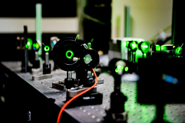
Details showing guiding of the 532nm laser beam used for NV spin polarization and readout. The beam is directed onto the quantum chip consisting of a diamond plate equipped with electrical contacts and MW strip lines for spin state manipulation (not shown).
Quantum applications and arrays
“Diamond-based qubits are unbeatable as room-temperature sensors for example for magnetic/electric field, temperature or molecules. If we do entanglement-based sensing, we can even further increase their sensitivity. For quantum computing applications, which typically require thousands of qubits, diamond qubits still face a few hurdles. The challenge is to deterministically produce NV centers with high probability. Currently, we can create them with a ~90% probability, but that number drops to ~65% when creating 4. If you go to thousands, the probability is very small… To solve this will require more research on all fronts, from materials to electronics to the full system.”
Milos Nesladek: “We now successfully demonstrated electrically-read entangled qubits. The next step is to leverage the scalability of the basic electron-nucleus unit and create arrays. We are working on a chip with 4 NV centers, 50nm apart. If we can stably couple these 4 qubits to 5 nuclear spins, we have access to a 20-qubit system which can be operated at reasonably low temperatures (around 10K or even higher). Then it becomes interesting for many new applications, such as quantum simulators!”
Want to know more?
Read more details about the work of Milos Nesladek’s team in two recent papers that can be requested via this link (https://www.imec-int.com/en/about-us/imec-magazine/contact-form-imec-magazine):
Background information about diamond research at IMO-IMOMEC can be found here https://www.imec-int.com/en/imec-magazine/imec-magazine-may-2019/the-potential-of-artificial-diamond-from-drilling-heads-to-quantum-sensors
Biography Milos Nesladek
Prof. Milos Nesladek, PhD, obtained his MSc. degree from the Faculty of Mathematics and Physics, Charles University in Prague, and the PhD degree from the Czech Academic Sciences, in collaboration with KU Leuven in the field of electronic transport in semiconductors. He is a professor of physics at the University of Hasselt and a member of staff at IMO-IMOMEC, an imec research group at University of Hasselt. He is one of the pioneering scientists in the field of growth of CVD diamond crystals in all forms, being in that field for the last 30 years. Prof. Nesladek’s research topic deals with photoconduction in condense matter systems with emphasis on wide-bandgap semiconductors. An example of this research is the development of photoelectrically read solid state Q-bits in diamond based on paramagnetic spin centres. Prof. Nesladek has participated in a large number of EU projects ranging from basic physics to industrial development projects which, some of them, he has coordinated. Prof. Nesladek is member of several conference boards and he is the Belgian representative to the Quantum Community Network (QCN) of the Quantum Flagship. Prof. Nesladek published over 300 scientific papers and contributed to several books. He is associated editor of Diamond Related Materials
This acquisition further establishes Quantum Machines as the quantum company with the broadest global footprint,…
Supporting planned growth in InP silicon photonics technology Resolving all prior IP disputes between the…
Norwest leads the round with strategic participation from Snowflake Ventures, as Jedify addresses the AI…
Round brings total funding to $15 million from U.S., European and Israeli investors to support…
Quantum Machines achieves 99.5% median two-qubit gate fidelity when operating Rigetti Computing’s Novera™ superconducting QPU…
Unframe, the managed AI delivery platform for global enterprises, today announced it has crossed $100…