What is a serial link?
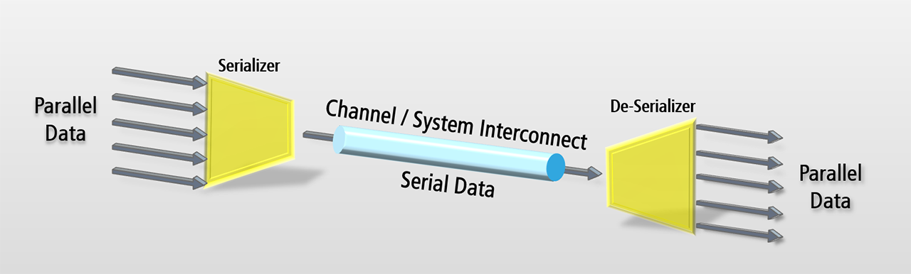
It’s an interface where data is serialized for high-speed data transmission. Serial data gets transferred from transmitter equalizer (serializer) to receiver equalizer (de-serializer). These are also known as “SerDes” components. The channel/ system connecting the SerDes components could consist of PCB, IC Package, connectors, capacitors, vias, backplanes, and/or cables.
The serial link interface will need to meet compliance standards set by special interest groups such as those focused on PCI Express® (PCIe®), High Definition Multimedia Interface (HDMI), or Serial Attached SCSI (SAS).
The advantages of serial links includes:
What are the challenges with serial link design and analysis?
The application of serial link design is everywhere: computers, smartphones, tablets, smart TVs, etc. Since the amount of data we push around is exploding, we have to find ways to transfer data faster! Are you still measuring data throughput in Gigabytes or Terabytes? Expand your mind. Today, we are talking about Exabytes, Zettabytes and Yottabytes!
Most interface standards double the speeds with the next generation. For example PCI Express® (PCIe®) Gen 3.0, which runs at 8 Gbps, is moving to version 4.0 of the spec which will run at 16 Gbps. Beyond that, we see interface specifications now running at 28 Gbps and some as fast as 56 Gbps. Some of these newer interface specifications also call for multi-level signaling (i.e., PAM-4) so that more data can be passed in a single unit interval.
What does that mean? No margin for error!
A small interconnect discontinuity can destroy the ability to meet compliance requirements for double-digit gigabyte interfaces. And there are a lot of factors PCB designers, IC Package designers, and signal integrity engineers have to take into account: design optimization, breaking out of pin fields, using curved traces to avoid “corners”, and optimizing via/ layer transitions to name just a few. Time domain simulation requires defining the proper stimulus, using the correct I/O model, extracting and connecting frequency domain S-parameter models, and checking simulation results against compliance requirements.
On top of all that, the challenge is to get results quickly when millions of bits must be simulated and extracting highly accurate interconnect models using full-wave 3D extraction is a long and tedious process.
What is the solution?
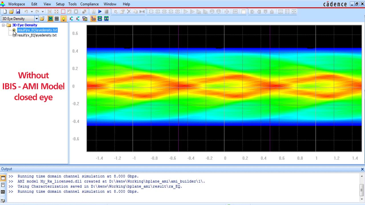
At speeds over 5 Gbps, signals require adaptive equalization. Simple tables (current vs. voltage) no longer suffice. Models must be represented in software algorithms and different equalization techniques such as FFE, CTLE, DFE must be incorporated into SerDes models.
IBIS-AMI is the recognized standard way to represent I/O models that allows simulators called channel simulators to simulate millions of bits (unit intervals) in minutes. It is simply not practical to simulate with transistor-level models using a traditional SPICE simulator to represent these various adaptive equalization algorithms. IBIS-AMI is the answer. But the creation of IBIS-AMI models can be challenging for companies that do not have programmers on staff to develop such models.
Fortunately, there is a complete solution that will helps SI engineers overcome these challenges:
In this video from EE Journal, news editor Amelia Dalton interviews Brad Griffin from Cadence Design System discussing serial link design and analysis challenges:
We hope you will watch and leave comments below. We are open to all kinds of discussions.
(Tool demonstrated is from Allegro® Sigrity™ System Serial Link Analysis Option)
Team Sigrity
The collaboration between Tower Semiconductor and Scintil Photonics offers a clear view into the future…
How virtual twins, accelerated computing and physics-based models are turning AI from smart software into…
For decades, cellular communication has relied on one almost unquestioned assumption: the base station is…
IBM (NYSE: IBM) today announced new results that its quantum computer can simulate real magnetic materials…
Arrow Electronics has announced the launch of a new evaluation platform, jointly designed in collaboration…
Siemens has unveiled Drivetrain Analyzer Onsite, a new on-premises analytics solution for industrial drive systems,…