

In this article we examine the rules and regulations governing control of EMI and the types of noise generated by switching power supplies to provide basic guidance for EMI mitigation, whether installed in other equipment as part of a larger system or in stand-alone applications.
Switching Power Supplies and EMC Standards
”Switching power supply” is a generic term that describes a power source with a circuit to convert dc to ac voltages that can be further processed into another dc voltage. Switching power supplies can be categorized as ac-dc power supplies (ac input) or dc-dc converters (dc input) since both incorporate dc to ac conversion for voltage change. By virtue of their inherent design characteristics, switching power supplies generate electromagnetic interference composed of signals of multiple frequencies. The dc-dc converter converts the input dc voltage to an ac voltage that can be stepped up or down via a transformer. Ac-dc power supplies also utilize high frequency circuits for voltage conversion. However, the internal ac voltage in either case is not a pure sine wave but frequently a square wave that can be represented by a Fourier series that consists of the algebraic sum of many sine waves with harmonically related frequencies.
These multiple-frequency signals are the source of conducted and radiated emissions which can cause interference to both the equipment in which the power supply is installed and to nearby equipment which may be susceptible to these frequencies.
Laws, Regulation, and International Cooperation –
The electro-magnetic spectrum has been widely used for broadcasting, telecom and data communications through intentional emissions of electro-magnetic fields. In order to protect the electromagnetic spectrum and ensure compatibility of collocated electrical and electronic systems, regulatory bodies have established standards to control conducted and radiated EMI in electronic equipment.
In Europe, one of the main standards is CISPR 22, adopted by the majority of the European Community, while in the US the FCC is the regulatory body. The FCC’s Part 15 rules categorize digital electronic equipment into Class A (designated for commercial, industrial, or business environments) and Class B (designated for use in a residential environment). Emission standards are more restrictive for Class B devices since they are more likely to be located close to other electronic devices used in the home.
CISPR 22 regulations have been harmonized with the FCC standards, and, with minor exceptions, can be used to certify digital electronic equipment. Harmonization requires that the same standard be used for both conducted and radiated emissions. Measurements made above 1 GHz must be made in accordance with FCC rules and limits as CISPR 22 has no specified limits for frequencies above 1 GHz and conducted / radiated emission limits specified in FCC Part 15 and CISPR 22 are within a few dB of each other over the prescribed frequencies.
EMC Testing and Compliance
EMC testing and compliance is performed according to the test procedure defined by the ANSI standard[1], which does not include either generic or specify product related limits on conducted and radiated emissions. It is worth noting that testing is done with the entire system, not just the power module. Even external power supplies that are in compliance with the regulations as a standalone product need to be tested with the end-system.
EMI/EMC Fundamentals Sources and Associated Frequencies
EMI can first be categorized as transient or continuous interference. Transient EMI arises when the source emits a short duration pulse of energy rather than a continuous signal. Sources can include switching electrical circuitry, as well as electrostatic discharge (ESD), lightning, and power line surges. Repetitive transient EMI can be caused by electric motors, gasoline engine ignition systems and continuous digital circuit switching.
Continuous interference can be further subdivided by frequency band.
Frequencies from a few tens of Hz up to 20 kHz are classified as audio, whereas radio frequency interference (RFI) occurs in a frequency band from 20 kHz and above (the level is increasing as new technologies emerge).
EMI Coupling
Coupling occurs either via conduction, radiation or induction. Conducted EMI emissions are measured up to 30 MHz. Currents at frequencies below 5 MHz are mostly differential mode, while those above 5 MHz are usually common mode.
The differential mode current is the expected current on a two wire pair, i.e., current leaves at the source end of the line and comes back on the return side of the line. The noise is measured on each line with respect to a designated reference point. Differential mode currents flow between the switching supply and its source or load via the power leads and these currents are independent of ground.
Common mode currents flow in the same direction in or out of the switching supply via the power leads and return to their source through ground. In many cases, common mode noise is conducted through parasitic capacitance in the circuit but can also flow through the capacitance between the case and ground.

Figure 1: Definition of Differential and Common Mode
Radiated coupling occurs when source and receptor (victim) act as radio antennas. The source radiates an electromagnetic wave that propagates across the open space between the source and the victim and is received by the victim.
Inductive coupling (either electrical or magnetic) is rare relative to conductive or radiated coupling and occurs where a short distance separates source and receptor.
Electrical induction occurs when a varying electric field exists between two adjacent conductors and causes a change in voltage across the gap. Whereas magnetic induction occurs when a varying magnetic field exists between two parallel conductors, inducing a change in voltage along the receiving conductor.
Characterization of the EMI problem requires understanding of the interference source and signal, the coupling path to the victim and the nature of the victim, both electrically and in terms of the significance of the malfunction. The risk posed by the threat is usually statistical in nature; so much of the work in threat characterization and standards setting is based on reducing the probability of disruptive EMI to an acceptable level rather than its assured elimination.
Conducted EMI
To effectively mitigate conducted emissions, it is imperative to address the differential mode noise and common mode noise separately.
Differential mode noise can usually be suppressed by connecting bypass capacitors directly between the power and return lines of the switching power supply. The power lines that require filtering may be those located at the input or the output of the switching power supply and the bypass capacitors on these lines need to be physically located adjacent to the terminals of the noise generating source to be most effective.
Attenuation of differential mode currents at lower frequencies around the fundamental switching frequency of the noise generating source may dictate that a much higher value of bypass capacitance is required, meaning a ceramic style capacitor would not be suitable. Ceramic capacitors up to 22 μF are only suitable filtering across the lower voltage outputs of switching power supplies but not for those supplies where 100 volt surges can be experienced. Instead, electrolytic capacitors, which have a high capacitance and voltage rating, should be employed.
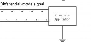
Figure 2: Differential Mode Filter Diagram
To suitably attenuate differential mode current both at the lower fundamental switching frequency as well as at the higher harmonic frequencies, differential mode input filters usually consist of a combination of electrolytic and ceramic capacitors.
Further suppression of differential mode currents can be achieved by adding an inductor in series with the main power feed to form a single stage L-C differential mode low pass filter with the bypass capacitor.
Conversely, common mode conducted currents are effectively suppressed by connecting bypass capacitors between each power line of the switching power supply and ground. These power lines may be at the input and/or output of the switching power supply.
Further suppression of common mode currents can be achieved by adding a pair of coupled choke inductors in series with each main power feed. The high impedance of the coupled choke inductors forces common mode currents through the bypass capacitors.
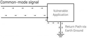
Figure 3: Common Mode Filter Diagram
Radiated EMI
Radiated EMI can be suppressed by reducing RF impedance and reducing the antenna loop area. This is achieved by minimizing the enclosed loop area formed by the power line and its return path.
The inductance of a printed circuit board track can be minimized by making it as wide as possible and routing it parallel to its return path. Similarly, because the impedance of a wire loop is proportional to its area, reducing the area between the power line and its return path will further reduce its impedance. Within printed circuit boards this area can be best reduced by placing the power line and return path one above the other on adjacent printed circuit board layers. Reducing the loop area between a power line and its return path not only reduces the RF impedance, but it also limits the effectiveness of the antenna because the smaller loop area produces a reduced electromagnetic field.
Furthermore, a ground plane located on the outer surfaces of the printed circuit board significantly suppresses radiated EMI, particularly if located directly below the noise-generating source.
And to further reduce radiated noise, metal shielding can be utilized, placing the noise-generating source within a grounded conductive housing, and interfacing to the clean outside environment is via in-line filters. Common mode bypass capacitors would also need to be returned to ground on the conductive housing.

Figure 4: Reduced Antenna Loop Area to Reduce Radiated Emissions
System-Level EMI Mitigation Techniques
Although most switching supplies are designed to meet applicable EMI standards as stand-alone modules, the system itself needs be designed to generate a minimum EMI profile to meet regulatory standards. Specific areas in the system design that are candidates for EMI mitigation practices include the signal lines, printed circuit boards (PCB), and solid state components.
Summary
Switching power supplies generate EMI because of their inherent design. Domestic and international regulatory bodies regulate these emissions through promulgation of rules and standards such as the FCC Part 15 rules and the CISPR 22 standard.
Power modules are one of many components within a system and EMI requirements, both radiated and conductive, apply to an overall electronic system. Since the EMI requirements apply to the overall system, significant effort must be expended on system design to limit noise.
Further information on EMI mitigation in power modules, including an application note, is available from the ac-dc power supplies and dc-dc converters pages of the CUI website.
[1] ANSI C63.4-2009 “Methods of Measurement of Radio-Noise Emissions from Low-Voltage Electrical and Electronic Equipment in the Range of 9 kHz to 40 GHz”


