
Many modern EW systems require low noise receivers capable of withstanding wide input power variations over a multi-octave bandwidth. These receivers are necessary to protect sensitive components from RF overdrive or to remove AM modulation from incoming signals. Further, multi-channel system designs and proximity to the receiver antenna generate requirements for low power and small package size. Applications include IFM and direction finding front ends, DRFM, and jammer systems. These systems must operate over a wide thermal range, and require a flat frequency response with low harmonic content under all operating conditions. ADI’s limiting amplifiers are ideal for many of these applications due to industry leading package size, electrical/RF performance, and ease of integration into higher level assemblies. A microwave limiting amplifier is a high gain, multi-stage amplifier that “limits” output power by successively compressing internal gain stages as input power increases. Gain stages compress from the output stage toward the input, with the design optimized to avoid overdriving individual gain stage under all operating conditions. Challenges associated with wideband limiting amplifier design include effective power limiting, thermal compensation, and frequency equalization over a multi-octave bandwidth. In addition, system requirements for low noise, low power, and a small package size add to the complexity of the design.
This paper reviews design considerations and techniques for a 2-18 GHz limiting amplifier with requirements for 45 ±1.5 dB gain, an operational temperature range of -40 to 85°C, less than 1.5 Watts DC, and a 40 dB limiting dynamic range. Limiting dynamic range is defined as the input power range over which RF output power is fixed. ADI offers a wideband 2-18 GHz limiting amplifier product, the HMC7891, that meets these requirements. This amplifier includes internal voltage regulation in a hermetically sealed connectorized package.
-

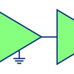
- Figure 1: Preliminary block diagram
-
- Figure 2: Block diagram, RF overdrive correction
-
- Figure 3: Simulated Pout vs frequency, RF overdrive correction
-
- Figure 4: Thermopad loss over temperature
-
- Figure 5: Block diagram, thermal compensation
-
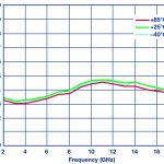
- Figure 6: HMC7891 simulated small signal gain over temperature
-
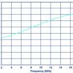
- Figure 7: Measured frequency equalizer loss
Construction and Amplifier Considerations
Microwave limiting amplifier design begins with down-selection of preferred construction methods and internal gain stage amplifiers. Hybrid chip-and-wire assemblies are often preferred over surface mount designs for high frequency applications in order to minimize detrimental performance impacts caused by package parasitics. Also, reliability of hybrid chip-and-wire assemblies is considered superior because hybrid assemblies are thoroughly inspected and are well suited to handle environmental stress. Further, these assemblies are small, lightweight, and easy to hermetically seal. Hybrid chip-and-wire assemblies consist of die form Monolithic Microwave Integrated Circuits (MMICs), thin film technology, and wire bondable passive components.
Primary considerations for selection of internal gain stages include operational frequency range, gain vs temperature, gain flatness, saturated harmonic content, and non-linear performance. A successful limiting amplifier design minimizes gain stages and unique part count to reduce thermal compensation and flatness challenges. Also, success largely depends on device maximum input power ratings and the compression characteristics of the selected gain stages. To complete a design with a 40 dB limiting dynamic range requirement, a minimum of four gain stages is recommended so that ideally each amplifier stage will operate no more than 10 dB compressed. Four gain stages should also be sufficient to achieve the 45 dB small signal gain requirement over temperature.
Wideband MMIC gain block amplifiers or low noise amplifiers (LNA’s) are good candidates for limiting amplifier designs due to their high gain and low power performance. A noise figure requirement will typically establish the need to utilize low noise amplifiers over gain block amplifiers. However, LNA gain stages can create design challenges due to their generally lower RF input power rating. An ideal gain stage device has a high maximum RF input power rating and can safely operate at high levels of compression.
Also important is the saturated harmonic content of each gain stage. Harmonic content requirements depend on the limiting amplifier’s application. For example, an application meant to generate a square wave output waveform needs to utilize gain stage amplifiers with low even harmonic output and strong odd harmonic output. To avoid corrupting the output waveform, it is useful to utilize the same part in all four gain stage locations. Finally, selected MMIC amplifiers must be unconditionally stable and ideally lack bias sequencing requirements to simplify the design.
The HMC462 is an ideal MMIC to complete a limiting amplifier design. The HMC462 is a self-biased LNA requiring a single +5V supply with greater than 13 dB gain, excellent 2-18 GHz gain flatness, and an average 2.5 dB noise figure. The device has an 18 dBm saturated output power level and can safely operate greater than 14 dB into compression across the frequency band. Maximum input power rating is nearly equivalent to the device’s saturated output power, making it ideal to operate in a cascaded series of gain stages. While second order harmonics are low, the MMIC has a strong, flat third order harmonic. Saturated DC power is less than 400 mW.
RF Budget Analysis
Following the selection of limiting amplifier gain stages, it is necessary to consider the RF system budget analysis. RF budget analysis examines the broadband frequency response and RF power levels at various test points within the limiting amplifier. Analysis must be completed to correct for worst case operational temperatures, gain slope, and a wide RF input power range. As discussed, the basic layout for a limiting amplifier with 40 dB limiting dynamic range is a cascaded series of four gain block amplifiers or LNAs. An ideal design utilizes only one or two unique amplifier part numbers to reduce power variations vs frequency and to minimize thermal/slope compensation requirements.
Figure 1 illustrates the first pass preliminary limiting amplifier block diagram prior to temperature correction and slope compensation. A recommended technique to complete the wideband limiting amplifier design is to:
1. Manage the limiting power dynamic range and eliminate RF overdrive conditions.
2. Optimize performance over temperature.
3. Complete the design by correcting the power roll-off and flatten the small signal gain.
4. A final minor correction may be necessary to revisit temperature compensation after frequency equalization has been included in the design.
-
- Figure 8: HMC7891 simulated frequency equalized small signal gain over temperature
-
- Figure 9: Block diagram, frequency equalization
-
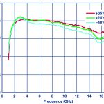
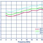
- Figure 10: HMC7891 simulated PSAT vs. frequency over temperature
-
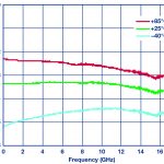
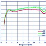
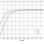
- Figure 11: HMC7891 measured PSAT vs frequency over temperature
-
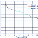
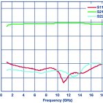
- Figure 12: HMC7891 measured gain and return loss
-
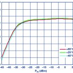
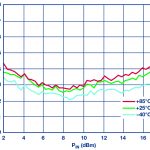
- Figure 13: HMC7891 measured Pout vs Pin at 2 GHz over temperature
-
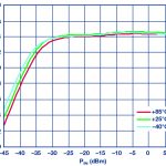
- Figure 14: HMC7891 measured Pout vs Pin at 10 GHz over temperature
Power Limiting
The primary issue with the preliminary design illustrated in Figure 1 is that RF overdrive will likely occur at the output gain stages as RF input power increases. RF overdrive will occur when the saturated output power of any gain stage exceeds the absolute maximum input of the succeeding amplifier in the lineup. Further, the design is susceptible to VSWR associated ripple and there is a strong potential for an oscillation to occur due to high, undamped gain within the small RF package.
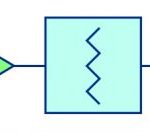
To prevent RF overdrive, diminish VSWR effects, and decrease the risk of an oscillation, add fixed attenuators between each gain stage to reduce power and gain. Eccosorb may also be required on the RF cover to eliminate oscillations. Sufficient attenuation is required to reduce the maximum input power of each gain stage below the MMIC’s rated input power level. It is necessary to include enough attenuation to accommodate top level input power margin and to account for thermal and part-to-part variations. Figure 2 illustrates the locations where RF attenuators are necessary within the limiting amplifier chain.
The ADI broadband limiting amplifier, HMC7891, utilizes four HMC462 gain stages and is designed to operate up to 10 dBm. Absolute maximum input power is 15 dBm. Each gain stage can withstand a maximum RF input of 18 dBm. Per the design step outlined in the preceding paragraph, attenuators were added between gain stages to ensure maximum amplifier input power levels do not exceed 17 dBm. Figure 3 illustrates the maximum power level at the input to each gain stage with fixed attenuators added to the design.
Thermal Compensation
The second step is to thermally compensate the design in order to increase the operational temperature range. A common thermal range requirement for limiting amplifier applications is -40 to 85°C. A rule-of-thumb gain variation formula of 0.01dB/degree/stage can be used to approximate the gain variability of a four stage amplifier design. Gain increases as temperature decreases and vice versa. Using ambient gain as a baseline, the total gain is expected to decrease 2.4 dB at 85°C and increase 2.6 dB at -40°C.
To thermally compensate the design, commercially available Thermopad temperature variable attenuators can be inserted in place of the fixed attenuators. Figure 4 illustrates test results of a wideband commercially available Thermopad attenuator. Based on Thermopad test data and the approximated gain variation, it is clear that two Thermopad attenuators are necessary to thermally compensate a four stage limiting amplifier design.
Deciding where to insert the Thermopads is an important decision. Due to the increased loss of Thermopad attenuators, especially at cold temperatures, it is good practice to avoid adding the components near the output of the RF chain in order to maintain a high limiting output power level. Ideal Thermopad locations exist between the first three amplifier stages, as highlighted in Figure 5.
Simulation results of ADI’s thermally compensated HMC7891 small signal performance is illustrated in Figure 6. Gain variation is reduced to a maximum of 2.5 dB prior to frequency equalization. This is within the ±1.5 dB gain variation requirement.
-
- Figure 17: HMC7891 measured second harmonic vs frequency at PSAT over temperature
-
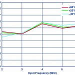
- Figure 16: HMC7891 measured NF vs frequency over temperature
-
- Figure 15: HMC7891 measured Pout vs Pin at 18 GHz over temperature
-
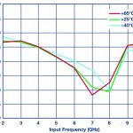
- Figure 18: HMC7891 measured Third Harmonic vs Freq at PSAT over Temperature
Frequency Equalization
The final design step is to improve gain flatness by incorporating frequency equalization. Frequency equalization compensates for the natural gain roll-off found in most wideband amplifiers by introducing a positive gain slope to the system. Various equalizer designs exist including passive GaAs MMIC die. Passive MMIC equalizers are ideal for limiting amplifier designs due to their small size and lack of DC and control signal requirements. The number of required frequency equalizers depends on the uncompensated gain slope of the limiting amplifier and the response of the selected equalizer. A design recommendation is to slightly overcompensate the frequency response to account for transmission line loss, connector loss, and package parasitics which have a greater impact on gain at higher frequencies than lower frequencies. Test results for a custom ADI GaAs frequency equalizer are found in Figure 7.
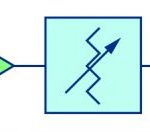
ADI’s HMC7891 limiting amplifier requires three frequency equalizers to correct the thermally compensated small signal response. Figure 8 illustrates the thermally compensated and frequency equalized simulation results of the HMC7891. Deciding where to insert the equalizers is critical for a successful design. Prior to adding any equalizers, it is important to remember that an ideal limiting amplifier evenly distributes maximum amplifier compression across all gain stages in order to avoid oversaturation. In other words, each MMIC should be equally compressed under worst case conditions.
At the current stage of the design, shown in Figure 5, equalizers can be added at the device input, in series with Thermopad attenuators, in place of the fixed attenuator, or at the device output. Adding equalizers to the limiting amplifier input decreases power at the first gain stage. As a result, stage 1 compression decreases. A decrease in gain stage compression is equivalent to a decrease in limiting dynamic range. Further, due to the equalizer’s attenuation slope, the limiting dynamic range disperses over frequency. Dynamic range decreases more at lower frequencies than at higher frequencies. To compensate for the decreased limiting dynamic range, the RF input power must increase. However, uniformly increasing input power adds to the risk of overdriving an amplifier gain stage due to the equalizer’s slope. It is possible to add an equalizer at the device input, but this is not an ideal location.
Next, adding an equalizer in series with the Thermopad will reduce the compression of the succeeding amplifier. This creates an uneven distribution of amplifier compression among gain stages and decreases overall limiting dynamic range. Equalizers in series with Thermopad attenuators are not recommended.
Third, substituting an equalizer (or equalizers) in place of the fixed attenuator changes only the compression level of the output stage amplifier. To minimize this change and avoid RF overdrive, the equalizer loss should be approximately equal to the fixed attenuation value being removed from the system. Further, as discussed earlier, adding equalizers prior to gain stages creates dispersion in limiting dynamic range vs frequency. To minimize this effect, substitute the minimum number of equalizers possible.
Finally, equalizers can be added to the device output. Output equalization reduces output power, but will not create limiting dynamic range dispersion. Output equalization does create a slightly positive output power slope, but this slope is offset by high frequency package and connector loss. A completed four stage limiting amplifier layout is illustrated in Figure 9.
Figure 10 illustrates the output power vs temperature simulation result for ADI’s HMC7891. The final design achieves 40 dB limiting dynamic range and has a simulated worst case output power variation of 3 dB under all operating conditions.
ADI Limiting Amplifier Test Results
Test results for the HMC7891 are illustrated in Figures 11–18. Results demonstrate the design was able to achieve 47 dB gain with a saturated output power of 13 dBm. The amplifier’s input power range is -30 to 10 dBm, for a limiting dynamic range of 40 dB. The unit was tested over an operational temperature range of -40 to 85°C. A photograph of the HMC7891 is shown inFigure 19. Though the HMC7891 was primarily designed as a limiting amplifier the small size and superior RF performance enable utility in various applications including use as a frequency tripler or as an LO amplifier. The design technique described herein can be used for future limiting amplifier designs with modifications to spec requirement such as frequency, output power, gain, NF, or limiting dynamic range.
“Thermopad” is a registered trademark of EMC Technology, Inc.


