

If you are a technology innovator, you’ll want your efforts and inventions to be protected from copying. Patents are a first line of defense, but enforcing them though litigation may be expensive and time-consuming. A more preemptive approach is to implement your IP as a package that is all but impossible to copy, e.g. as a dedicated application specific integrated circuit (ASIC). Due to the long-term trend of price reductions for advanced (but not necessarily leading-edge) foundry technologies, it has become an attractive and cost-effective option for innovative SME’s to design such an ASIC.
Patents are your first line of protection, but can you enforce them?
The origin of patents may be traced back in time to Queen Elizabeth I of England who granted monopoly privileges to businesses by means of letters patent, meaning public documents. These ultimately enabled investors to form business ventures to explore business opportunities in the New World.
Starting out as a royal permission for the exclusive commercialization of land, patents have since evolved to become legally enforceable rights that provide exclusive control over the production and sale of Intellectual Property (IP), otherwise known as inventions.
A company who implements an invention without the permission of the patent holder is said to have infringed the patent. But it is up to the owner of the patent to discover the infringement and initiate court proceedings. For some technology companies, especially startups and SME’s, this may place an important burden on their efforts to bring their innovative products to market. For one, as an innovator, you often have financial constraints, especially because you investment costs – particularly R&D – are incurred before they have any prospect of revenues.
Your PCBs will be reverse engineered, fast
 At some point, intellectual property in the technology domain has to be physically implemented and manufactured. This still often takes the form of a PCB (printed circuit board) comprised of a variety of mounted discrete components, which may include a power supply, Bluetooth functionality and a microcontroller.
The problem with this widely-used approach is illustrated by an internet search query for the phrase “PCB reverse engineering”. This returns over 20,000 hits and clearly represents an established international industry.
The copying process begins by stripping all the parts off the board to identify parts. The PCBs can then be delaminated into their individual layers and imaged in order to reconstruct a schematic diagram of the board. This reverse engineering industry also includes companies that offer to extract the code from your microcontrollers; so not even the firmware running on the boards is safe from cloning.
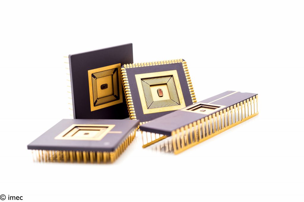
ASICs, at least modern ones, turn out to be your best safeguard
These issues have led technology companies to revert to ASICs (Application Specific Integrated Circuits) as a means of physically implementing and protecting their IP.
But in older IC technologies, meaning those with one or two metal layers and 1um-2um critical dimensions, this still didn’t prove secure. After package removal (also known as “depotting”) all features could easily be seen using optical imaging equipment to take high resolution images. The cloning process could then proceed using similar methods as PCB cloning.
With more recent foundry fabrication technologies using critical dimensions of 180nm and less, this is much, much more difficult. This is not only due to the difficulties of imaging these sub-wavelength dimensions using optical, wide-field microscopes, there are also many more metal interconnect layers, larger numbers of logics gates, plus analog blocks, Radio Frequency (RF) blocks, memory, MEMs, inductors and other devices integrated on-chip. All these factors combine to make ASIC cloning extremely time consuming and ultimately uneconomic for all but the biggest companies.
 A typical example of a fast-innovating technology company is Belgium-based Van de Wiele, a global leader in advanced equipment and specialized services for the textile manufacturing industry. Van de Wiele has repeatedly suffered from reverse engineering of the boards used to control yarn systems. R&D manager Hans Desmet admits that “the first machine we released that used ASIC controllers was the first one that was not copied”.
The IoT offers a huge opportunity for nimble, fast-moving innovation
The accelerating trend of technology innovators to use ASICs for IP protection has been driven by the recent confluence of three key drivers.
First, there has been an explosion in applications for what has been loosely grouped under the heading of the Internet of Things (IoT). This has enabled companies with leaner decision making cycles and closer connections to the latest trends to move more rapidly to market than larger companies.
Second, while the volume of chips needed to address the IoT market is huge, the fragmentation of the market into a large number of potential IoT applications means that the production volumes of individual designs will be relatively small. This makes it difficult for large companies to compete on their ability to ramp large production volumes. In many ways large companies have outsourced innovation to technology SMEs.
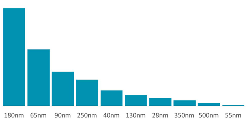
Finally, and perhaps most importantly, one of the key characteristics of IoT applications is that they require advanced but not necessarily leading-edge silicon technology. This is primarily due to the fact that some form of wireless communication is required and the corresponding analog circuit blocks to implement this functionality do not benefit very much from aggressive feature size scaling. The costs for implementing production prototypes with such foundry technologies are extremely low. Using imec IC-link’s multi-project wafer (MPW) service, a company can produce a prototype run of a 25mm2 ASIC in the extremely popular 180nm technology with 45 samples for as little as $16,000.
Here comes substream innovationNumber of ASIC projects as a function of technology node. Source imec IC-link database.
The use of ASICs coupled with low-cost foundry technologies is giving rise to a new wave of technology–based innovation. But this would not be possible if the ASICs would not protect the IP. Together, accessible low-cost technologies and IP protection have enabled SMEs with great ideas to gain access to lucrative, high growth, global markets. We refer to this as substream innovation and like to think it would be easily recognizable to those earlier business adventurers looking for opportunities in the New World.
Phill Christie is a Principal Scientist and leads the Business & Technology Strategy Group at imec IC-link. You can reach him at Phillip.Christie@imec.be


