
Introduction
Deep in the darkest depths of ARM®’s Cambridge campus reside a small team of engineers whose job it is to envision and create forward thinking technology demonstrations based on ARM. That team goes by the name of Applied Systems Engineering for which I am an Engineer, concentrating on the electronic elements of the demos that we create.
Last year we designed and developed a demonstration of an ARM-based, end-to-end, Internet of Things (IoT) application to demo at some of the biggest electronics trade shows around the world. We called this demo Sensors to Servers. Over a three part blog my colleague ericgowland talks about how we took the concept and made it a reality (part 1 with video, part 2, part 3).
To briefly recap, Sensors to Servers is a demo which collects and visualises live data from around our trade show booths. To make this happen we instrument our booths with a network of sensor nodes featuring ARM Cortex®-M4 based microcontrollers from NXP Semiconductors. These sensors nodes are strategically positioned around the booth and report their findings to an ARMv8-A based 64-bit server from Applied Micro®. The key to bringing this demo together is the ARM mbed™ IoT Device Platform. The sensor node application software was written on top of mbed “Classic” (v2.0) and the data was collect by our server using thembed Device Server software.
Over the next two blogs I will show you how the demo evolved from a stack of development boards to a cloud hosted application which we deployed simultaneously at Mobile World Congress™ and Embedded World 2016. For this instalment we will concentrate on how we took the original sensor nodes and updated them with new custom hardware.
Custom Sensor Nodes
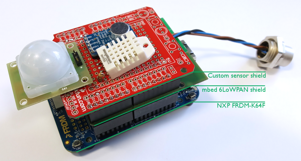
When we were originally creating this demo we selected one of the many available mbed development boards to use as the basis of our sensor nodes. For rapid prototyping (and other reasons) we selected the NXP FRDM-K64F which gave us Arduino compatible headers, from this we could stack shields together that would very quickly give us the functionally which we required. This was great; the speed at which we could develop and test was instrumental in meeting our deadline for a stable demo. We went on to use this setup when we deployed Sensors to Servers in its first few outings.
Original sensor node:


Although brilliant for development and testing the stack of shields was far from an elegant solution and frankly an ugly addition to our skilfully crafted trade show booths. We therefore started working on custom sensor nodes which would give us the same functionality and be software compatible while being far more professional and pleasing on the eye.
So where did we start? Documentation; we had the schematic for our sensor shield but we needed to know exactly what hardware we were using on the FRDM-K64F board and mbed 6LoWPAN shield so we could replicate it. We downloaded the design files for the FRDM-K64F from the NXP website (schematic, BOM and Gerber files). The mbed 6LoWPAN shield is simply a 2.4 GHz IEEE 802.15.4 transceiver module routed to Arduino R3 standard headers. We looked up the part number of the module and found the datasheet and schematic for it. Using these, a keen eye and a continuity tester it didn’t take us long to reverse engineer the shield. Now we had all of documentation we needed we could start designing our custom, 4 layer PCB.
Design & Assembly
Using CadSoft EAGLE PCB design software we put together our schematic. We studied the documentation we had gathered and carefully worked out what components we needed using the documentation as a reference. We tried to copy as many components that we needed from the original setup as we could. Once we were confident in our design we laid out and routed our PCB and sent the design files off to Eurocircuits, a PCB pooling company for a quick turnaround run of test boards.
The first revision of the board didn’t quite work out as we liked. After we hand assembled some boards and corrected the inevitable mistake or two we found that the Ethernet signal quality degraded significantly over only a short distance, well short of the 100 meter standard. We went back to the drawing board and re-worked the layout of the Ethernet MAC and jack, particularly focusing on minimising cross-talk by carefully sculpting the ground and power planes of the PCB. The revised spin of the PCB came back working perfectly.
We decided that 40 nodes would be enough for our needs and none of our team fancied the pain staking job of assembling them by hand (unsurprisingly!) so we needed to find a company that would assemble them for us. After tonnes of phone calls and quotes we luckily found a small assembly house with a pick-and-place machine a mere 4 miles away. After liaising with the assembly house we ordered our final PCBs in panels of 12 so the pick-and-place machine could do its job. 48 hours after dropping off the PCBs and components the now completed nodes were back in our hands and working perfectly much to our relief. One last touch was required; a laser cut acrylic protective casing and we were done!
Hardware

Power supply: We choose to power the nodes using a micro-USB connector with a standard 5V USB input. We required three voltage rails to power all of the various components, 3.3V, 5V and 12V. To step-down the 5V input we selected a fixed 3.3V low-dropout (LDO) voltage regulator. To step-up the 5V input to 12V we included a boost converter IC and supporting circuity. Power consumption wasn’t really a big concern for the nodes as they are powered by either USB chargers or mobile phone power banks.
Microcontroller (MCU): The target MCU was plucked straight from the FRDM-K64F board. The part in question is from the Kinetics K Series from NXP Semiconductors. It features a Cortex-M4 processor with a digital signal processor (DSP) and floating-point unit (FPU), 1 MB of flash, 256 KB of SRAM, Ethernet MAC and many other peripherals. Although capable of being clocked at a maximum 120 MHz the MCU is clocked at 50 MHz. This is because the clock signal is derived from an external Ethernet PHY as per the FRDM-K64F board.
Programming Interface: We opted to stray from the mbed Hardware Development Kit (HDK) specification and not include an on-board CMSIS-DAP interface. The CMSIS-DAP interface provides provisions for drag and drop programming and USB virtual COM port. We did this to save board space and BOM costs. So how did we program the nodes? We used the CMSIS-DAP interface on the FRDM-K64F board as it is ready to program and debug the target MCU. A simple modification on the FRDM-K64F board allowed us to program the nodes with a 10-pin ribbon cable:

Connectivity: To communicate with our server we included wireless and wired options, 6LoWPAN and Ethernet respectively. Large trade shows are notoriously bad for having a crowded and noisy RF environment. To ensure that the demo functions in all scenarios we made sure we could fall back on wires if needs be. The 6LoWPAN functionality came from the same 2.4 GHz IEEE 802.15.4 transceiver module as on the mbed 6LoWPAN shield.
Sensors: We refined our choice of sensors from our original setup from the experience we gained in the demos early deployments. The PIR sensor was dropped in favour of an accelerometer however, we kept the option to reinstate it. We found that measuring the vibrations of a table was a more effective way of determining presence in a meeting room than trying to position a small PIR sensor effectively. We swapped the temperature sensor for one which we could surface mount and it was placed in corner of the board within an isolated area for greater accuracy. The microphone was re-used, however we integrated it and it’s amplifier into the PCB instead of using the module. We added an optional 4-pin M12 connector to the board (number 11 below) which allows us to attach the same laser door trip sensor as we used previously. We only fitted the connector to the required nodes.
Components
The image below highlights all of the major components we used on our custom sensor nodes:

- Temperature sensor: Measurement Specialties™ HTU21D
- Microphone: CUI CMA-4544PF-W
- Boost converter, 12V: Texas Instruments™ LM2731
- USB UART interface: FTDI FT232R
- Low-dropout voltage regulator, 3.3V: Microchip® MCP1824T
- Micro-USB receptacle
- Accelerometer and magnetometer: NXP FXOS8700CQ
- 2.4 GHz IEEE 802.15.4 transceiver: Atmel® ATZB-RF-233-1-C
- Ultrasonic proximity sensor module: MaxBotix® MB1014
- MCU: NXP Kinetis K64 (MK64FN1M0VLL12)
- Door trip 4-pin M12 connector (fitted when needed)
- Programming interface, 10-pin Cortex debug connector
- Ethernet jack with magnetics: WIZnet RB1-125BAG1A
- Microphone amplifier: Maxim Integrated™ MAX9814
- Ethernet PHY: Microchip KSZ8081
Conclusion
I hope you enjoyed reading about some of the work that goes on to bring ARM demonstration to life. Stay tuned for the next instalment where I will talk about how we modified the demo for cloud hosting which we deployed simultaneously at Mobile World Congress and Embedded World 2016.
https://community.arm.com/groups/internet-of-things/blog/2016/04/19/sensors-to-servers-from-prototype-to-custom-hardware


