For anyone familiar with 3D printing and printed circuit boards (PCBs) it’s difficult to imagine a future where PCBs are not 3D printed. 3D printing promises to make PCB manufacturing faster, easier and more innovative. It is only recently however that Printed Electronics and 3D printing technology has started to catch up with imagination.
First a brief introduction to the world of 3D printing, or as it’s more properly known ‘additive manufacturing’. Nowadays it comprises a range of different competing processes that use heat, lasers, inkjet deposition or other techniques to add different materials, layer by layer, to build new or to add to existing objects. Each process has advantages and disadvantages in terms of precision, materials, end-product durability and flexibility in terms of the objects and shapes that can be supported. As a rule there is a correlation between price, resolution and range of supported materials.
Developing Materials for Electronics
To 3D print PCBs the systems have to be able to print conductive traces, which is the domain of Printed Electronics. This is an advanced technological area which involves the development of conductive materials suited to a range of different substrates. Basic connections can be embedded in objects by 3D extrusion printers using conductive filaments. These contain conductive polymers, carbon nano-tubes or other conductive materials. However, the end result, using current technologies, is a low resolution, point-to-point conductive trace that struggles to cope with the electrical requirements of professional circuits.
For higher resolution and acceptable conductivity, more advanced printing solutions are required. The nano-ink industry is currently providing formulations to meet this challenge in the form of various silver nanoparticle inks. These inks are suspensions of nanometer sized silver particles that, after printing, need to be cured either chemically, by light or by heat. Once cured, the particles coalesce to form a conductive solid silver trace. The technology is now developed enough that silver nanoparticles are emerging as a mature technological solution to printing electronics. That is not to say that all silver nanoparticle inks are the same, nano-ink development itself is a very advanced field. Silver may be an expensive metal to use but given that traces are so fine not much is needed. The performance justifies the cost.
Copper ink would be clearly preferable from a cost perspective but copper ink is not currently a mature enough technology. Copper is much harder to print with as oxidation issues mean that the ink isn’t as easy to make or use and the end results are not robust. Carbon nano-tubes and other exotic materials may well offer alternatives in the future also.
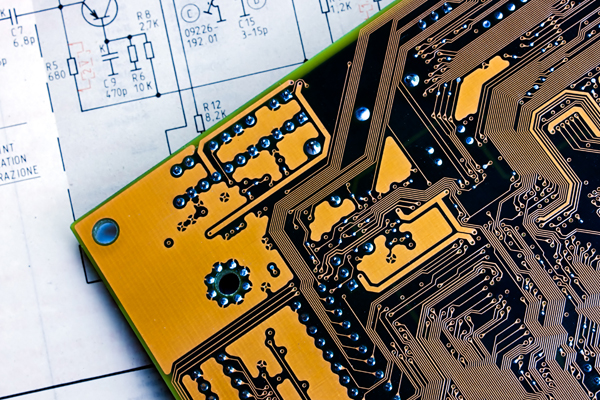
3D Printing Professional Multi-Layer PCBs
On one hand PCBs are multilayered which implies they are well suited to additive manufacturing. On the other hand the multiple materials, conductivity requirements and exacting precision present serious technological challenges.
To rise to the challenge of making proper multilayer PCBs the conductive traces clearly have to be printed in such a way that they are precise enough, conductive enough and robust enough to do the job reliably. Inkjet deposition is likely to be the first true
3D printing process to provide this technology for professional multilayered PCBs.
 Having solved the printing of advanced inks to give precise conductive traces the next step in order to 3D print a PCB is to print the substrate. For traditional rigid boards the substrate ink material needs to be inkjet printable, e an excellent insulator and offer rigidity that is comparable to standard FR4. Flexible boards are another field and require a different combination of substrate and conductive ink formulations. Each substrate requires its own ink specifications to ensure adhesion, precision and compatibility with the relevant ink curing stage.
If nano-materials can be engineered to meet the requirements of a PCB the next challenge is how to manage the printer. The software has to be able to process Gerber files which are intended for a 2D manufacturing environment. This would allow the 3D printer to print the substrate to the required thickness, to leave and fill holes where vias are required and so on.
The only company currently dedicated to 3D printing professional multilayer rigid PCBs is Nano Dimension. The company, which is listed on the Nasdaq and Tel Aviv stock exchange (NNDM), is developing a 3D inkjet printer that will offer in-house rapid-prototyping of professional multilayer PCBs to be printed in-house. To this end the company has formulated and makes its own nano-inks. To make a multi-layer PCB Nano Dimension’s printer will print a proprietary silver nano-particle ink for the conductive trace and another proprietary nano particle dielectric ink for the insulating layer. The company promises a trace width of 3-4 Mil.
It is early days for the 3D electronics revolution but it’s clearly coming. If all of these elements; 3D printer, inks and software come together then there is no reason that PCBs shouldn’t be 3D printed. 3D printing can lead to dramatically faster in-house development, protect IP in development, reduce waste and even inject more design innovation and creativity with PCBs that can not be produced in any other way.
For prototypes and very small-batches, 3D printing may be just around the corner. First printers will deliver in-house prototyping solutions that change the way products are developed however, as is the case in other industries it is unlikely that 3D printers will replace efficient mass-production processes anytime soon. Whether 3D printing completely replaces traditional manufacturing processes remains to be seen. There are those that dream of a 3D printer that can print multi-material objects with completely embedded HD circuits and no traditional PCB at all.