
Introduction
It goes without saying that PC board layout determines the success or failure of every power supply design. It sets functional, electromagnetic interference (EMI), and thermal behavior. While switching power supply layout is not black magic, it is often overlooked until it is too late in the design process. Therefore, having a proven way to mitigate the potential threats from EMI generation from the onset can ensure a quiet and stable power supply. While many switch mode power supply designers are familiar with the design complexities and nuances of switch mode supplies, there are simply not enough designers in many companies to get all the designs done for all of their project needs. They are retiring and leaving the industry! So, how does this problem get solved?
Well, for one thing, more and more digital designers are being asked to take on switch mode power supply designs, if for no other reason than there are simply not enough analog power supply designers to get the job done! While it is safe to say that most digital designers know how to design with a simple linear regulator, not all of their power requirements are step-down (buck mode). In fact, many are step-up mode (boost) or even a buck-boost topology (buck and boost modes combined).
Clearly, an obvious question facing many electronic systems manufacturers is this: How will all the switch mode power supply circuits needed in my systems get finished?
Solving a Design Resource Shortfall
During the course of this discourse, I will go over some of the basics of buck regulator operation including how high di/dt and parasitic inductance in the switcher hot loop cause electromagnetic noise and switch ringing. And then we will see what can be done to reduce the high frequency noise. I will also introduce ADI’s Power by Linear™ Silent Switcher® technology, including how it is constructed, and demonstrate how it helps solve EMI problems without any compromises. This will also include how Silent Switcher devices work.
I will also give an overview of Silent Switcher packaging and layout and discuss how these can enhance the overall performance of the step-down converters. Moreover, I will show how to achieve a higher level of integration of our Silent Switcher device by demonstrating how this technique can be incorporated into our μModule® regulators. These provide simple and easy to use solutions for those users who are not sophisticated in switch mode power supply design techniques.
Basic Buck Regulator Circuit
One of the most basic power supply topologies is the buck regulator, as shown in Figure 1. EMI starts off from the high di/dt loops. The supply wire, as well as the load wire should not have high ac current content. Accordingly, the input capacitor, C2 should source all the relevant ac to the output capacitor, C1, where any ac ends.
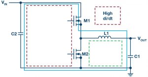
Figure 1. A synchronous buck regulator schematic.
Still referring to Figure 1, during the on cycle with M1 closed and M2 open, the ac follows in the solid blue loop. During the off cycle, with M1 open and M2 closed, the ac follows the green dotted loop. Most people have difficulty grasping that the loop producing the highest EMI is not the solid blue nor the dotted green. Only in the dotted red loop flows a fully switched ac, switched from the zero to I peak and back to zero. The dotted red loop is commonly referred to as a hot loop since it has the highest ac and EMI energy.
It is the high di/dt and parasitic inductance in the switcher hot loop that causes electromagnetic noise and switch ringing. To reduce EMI and improve functionality, one needs to reduce the radiating effect of the dotted red loop as much as possible. If we could reduce the PC board area of the dotted red loop to zero and buy an ideal capacitor with zero impedance, the problem would be solved. However, in the real world, it is the design engineer who must find an optimal compromise!
So where does all this high frequency noise come from anyway? Well, in electronic circuits, the switching transitions coupled though parasitic resistors, inductors, and capacitors create high frequency harmonics. So, knowing where the noise is generated, what can be done to reduce the high frequency switching noise? The traditional way to reduce noise is to slow down the MOSFET switching edges. This can be accomplished by slowing the internal switch driver or by adding snubbers externally.
However, this will reduce the efficiency of the converter due to increased switching loss—especially if the switcher is running at a high switching frequency of, say, 2 MHz. Speaking of which, why would we want to run at 2 MHz? Well, for several reasons actually:
- It enables the use of smaller (size) external components such as capacitors and inductors. For example, every doubling of switching frequency is a halving of inductance value and output capacitance value.
- In automotive applications, switching at 2 MHz keeps noise out of the AM radio
Filters and shielding can also be employed, but this costs more in terms of external components and circuit board area. Spread spectrum frequency modulation (SSFM) could also be implemented—this technique dithers the system clock within a known range. SSFM helps to pass the EMI standards. The EMI energy is distributed over the frequency domain. Although the switching frequency is most often chosen to be outside the AM band (530 kHz to 1.8 MHz), unmitigated switching harmonics can still violate stringent automotive EMI requirements within the AM band. Adding SSFM significantly reduces EMI within the AM band as well as in other regions.
Or, one could simply use ADI’s Silent Switcher technology instead since it delivers on all the points outlined with no trade-offs:
- High efficiency
- High switching frequency
- Low EMI
Silent Switcher Technology
A Silent Switcher device breaks the trade-off between EMI and efficiency by not needing to slow down the switch edge rates. But how can this be accomplished? Consider the LT8610, as shown on the left side of Figure 2. It is a 42 V input capable, monolithic (FETs inside) synchronous buck converter that can deliver up to 2.5 A of output current. Notice that it has a single input pin (VIN) at its top left corner.
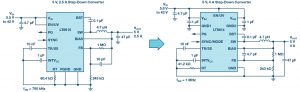
Figure 2. How to make an LT8610 into a Silent Switcher device—the LT8614.
However, when contrasting the LT8610 to the LT8614 (a 42 V input capable, monolithic synchronous buck converter that can deliver up to 4 A of output current), one can see that the LT8614 has two VIN pins and two ground pins on the opposite side of the package. This is significant, since it is part of what makes it silent switching!
How to Make a Switcher Silent
So how can we do what we do? Placing two input capacitors on opposite sides of the chip between the VIN and ground pins will cancel the magnetic fields. This is highlighted in the slide with the red arrows pointing to the capacitor placement, both on the schematic and the demo board, as shown in Figure 3.
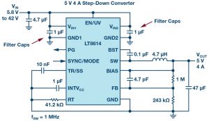
Figure 3. Diagram of the LT8614 showing the filter caps between VIN and ground pins on opposing sides of the IC.
The LT8614 in More Detail
The LT8614 incorporates Silent Switcher capability. With it, we were able to reduce the parasitic inductance by using copper pillar flip-chip packaging. Furthermore, there are opposing VIN, ground, and input caps to enable magnetic field cancellation (right-hand rule applies) to lower EMI emissions.
Reducing the package parasitic inductance is achieved by eliminating the long bond wires of a wire-bonded assembly technique, which induces parasitic resistance and inductance. The opposing magnetic fields from the hot loops cancel each other out and the electric loop sees no net magnetic field.
We compared the LT8614 Silent Switcher regulator against a current state-of-the-art switching regulator, the LT8610. Testing was performed in a GTEM cell using the same load, the same input voltage, and the same inductor on the standard demo boards for both parts. We found that a 20 dB improvement is made when using the LT8614 compared to the already very good EMI performance of the LT8610, especially in the more difficult to manage higher frequency areas. This enables simpler and more compact designs where the LT8614 switching power supply needs less filtering and distance compared to other sensitive systems in the overall design. Furthermore, in the time domain, the LT8614 exhibits very benign behavior on the switch node edges.
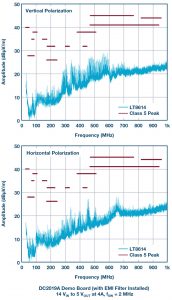
Figure 4. The LT8614 radiated EMI performance passes the most stringent CISPR 25 Class 5 limits.
Further Enhancements to Silent Switcher Devices
Although the LT8614 has impressive performance, we did not stop trying to improve upon its performance. Accordingly, the LT8640 step-down regulator features Silent Switcher architecture designed to minimize EMI/EMC emissions while delivering high efficiency at frequencies up to 3 MHz. Assembled in a 3 mm × 4 mm QFN, the monolithic construction with integrated power switches and inclusion of all necessary circuitry yields a solution with a minimal PCB footprint. Transient response remains excellent and output voltage ripple is below 10 mV p-p at any load, from zero to full current. The LT8640 allows high VIN to low VOUT conversion at high frequency with a fast minimum top switch on-time of 30 ns.
To improve EMI/EMC, the LT8640 can operate in spread spectrum mode. This feature varies the clock with a triangular frequency modulation of 20%. When the LT8640 is in spread spectrum frequency modulation mode, a triangular frequency modulation is used to vary the switching frequency between the value programmed by RT to approximately 20% higher than that value. The modulation frequency is approximately 3 kHz. For example, when the LT8640 is programmed to 2 MHz, the frequency will vary from 2 MHz to 2.4 MHz at a 3 kHz rate. When spread spectrum operation is selected, Burst Mode® operation is disabled, and the part will run in either pulse-skipping mode or forced continuous mode.
Nevertheless, despite all we stated in our Silent Switcher data sheets, such as showing the schematic and layout recommendations, as well as the input capacitors being placed as close as possible to the IC on both side—some of our customers still make mistakes. Furthermore, our in-house engineers were spending too much time fixing our customer’s PCB layouts. So, our designers came up with a brilliant solution to this problem—the Silent Switcher 2 architecture.
Silent Switcher 2
With Silent Switcher 2 technology, we simply integrated the capacitors inside a new LQFN package: VIN caps, IntVCC, and boost caps—allowing for placement as close as possible to the pins. The benefits included all the hot loops and ground planes inside, with all of this resulting in lower EMI. Fewer external components meant a smaller solution footprint. Furthermore, we also eliminated PCB layout sensitivity.
As shown in Figure 5, you can see how the schematics for the LT8640 and LT8640S differ. And, the marketing breakthrough was to give the new, higher integrated version with internal caps an “S” suffix. Because it is more “silent” than the 1st generation!
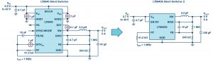
Figure 5. The LT8640S is a Silent Switcher 2 device with a higher level of integration of capacitors.
Silent Switcher 2 technology enables better thermal performance. The large multiple ground exposed pads on the LQFN flip-chip package facilitate the pulling of heat out of the package and into the PCB. We also get higher conversion efficiency since we have eliminated the high resistance bond wires. The EMI performance of the LT8640S easily passes the radiated EMI performance CISPR 25 Class 5 peak limits with a wide margin.
The Next Step: Everything Integrated with Silent Switcher 2 μModule Regulators
Silent Switcher technology is so compelling that we elected to incorporate it into our μModule regulator product line. In this form factor, everything is integrated inside a single package and provides the user with simplicity, reliability, performance, and high power density. The LTM8053 and LTM8073 are micromodule regulators where everything is virtually integrated with just a few capacitors and resistors external to them.
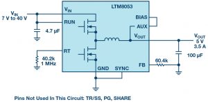
Figure 6. The LTM8053 Silent Switcher 2 μModule.
Summary
In conclusion, Silent Switcher capabilities and benefits will make it easier for your switch mode power supply designs to pass the various noise immunity standards such as CISPR 32 and CISPR 25. They can do this easily and effectively due to their following attributes:
- High efficiency conversion at greater than 2 MHz switching frequency with minimum impact on conversion
- Internal bypass capacitors reduce EMI radiation and provide for a more compact solution
- PCB layout sensitivity is essentially eliminated with Silent Switcher 2
- Optional spread spectrum modulation helps mitigate noise sensitivity.
- Using Silent Switcher devices saves on PCB area and can also reduce the number of layers
Tony Armstrong [tony.armstrong@analog.com] is currently the product marketing director for Analog Devices’ Power by Linear product group. He is responsible for all aspects of power conversion and management products from their introduction through obsolescence. Prior to joining ADI, Tony held various positions in marketing, sales, and operations at Linear Technology, Siliconix Inc., Semtech Corp., Fairchild Semiconductors, and Intel. He attained his B.S. (Honors) in applied mathematics from the University of Manchester, England


