


t this week’s 2018 Symposia on VLSI Technology and Circuits, imec, the world-leading research and innovation hub in nanoelectronics and digital technology presented considerable progress in enabling germanium nanowire pFET devices as a practical solution to extend scaling beyond the 5nm node. In a first paper, the research center unveiled an in-depth study of the electrical properties of strained germanium nanowire pFETs. A second paper presents the first demonstration of vertically-stacked gate-all-around highly-strained germanium nanowire pFETs.
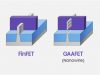
“With a number of scaling boosters, the industry will be able to extend FinFET technology to the 7- or even 5nm node,” says An Steegen, EVP at imec’s Semiconductor Technology and Systems division. “Beyond, the gate-all-around (GAA) architecture appears as a practical solution since it reuses most of the FinFET process steps. But one important challenge of using lateral nanowires is the significant decrease of the channel cross-section compared to conventional FinFETs. To improve the drive per footprint, several nanowires have to be stacked, but this comes with a serious penalty of increased parasitic capacitance and resistance. A solution is to replace the silicon nanowires by a high-mobility channel material such as germanium (Ge), providing the necessary current boost per footprint”, adds Steegen, “These new studies show that solution is indeed feasible, reaching the cost, area and performance requirements for nodes beyond 5nm.”
The first study of high-performing strained Ge nanowire pFETs gives insight in the device performance these new devices may offer for high-end analog and high-performance digital solutions. One conclusion is that dedicated optimizations of key process steps make these devices a serious contender for the GAA technology. The second paper reports on Ge GAA FETs with single nanowires, achieving a performance that matches state-of-the-art SiGe and Ge FinFETs. Moreover, for the first time, strained p-type Ge GAA FETs with stacked nanowires were demonstrated on a 14/16nm platform. The GAA nanowire technology appears as a promising high-performance solution for future nodes, provided that the junctions are further optimized.
“These complimentary studies establish germanium GAA nanowire technology as a valid contender for the sustained scaling that will be required to fulfill the requirements for the data-driven IoT-era requiring huge computational power,” concludes Steegen.
These results will be presented on June 20 at the VLSI Technology Symposium, in session T8: Advanced FinFET and GAA. This research is performed in cooperation with imec’s key program partners including GlobalFoundries, Huawei, Intel, Micron, Qualcomm, Samsung, SK Hynix, Sony Semiconductor Solutions, TOSHIBA Memory, TSMC and Western Digital.