

Leti, a French research institute at CEA Tech, and Mapper Lithography BV, the leading provider of maskless direct-write lithography equipment for the semiconductor industry, recently announced a low-cost cybersecurity breakthrough that allows encrypting unique codes directly on individual chips.
This technology provides a novel way to secure private information, devices, business exchanges, cloud data, etc., in the massive data exchanges enabled by the Internet of Things (IoT). Several technological solutions, such as software or fuse or physical unclonable function (PUF) strategy, are available, but present their own safety limitations. Indeed, none of these solutions can directly and deeply spread security codes into the hard IP core of the devices, a technique that significantly enhances anti-piracy efficiency in the final product. The encryption approach offered by maskless lithography opens a new technology era in the field of cyber-security.
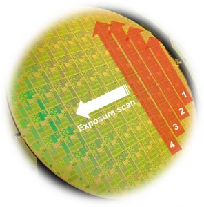

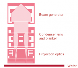
Figure 1: FLX-1200 platform dedicated for pilot R&D picture and basic operation schemes
Mapper Lithography has introduced its first pilot R&D platform, the FLX–1200 platform, which is initially designed to reach throughput of one 300mm wafer per hour (wph) for a wide range of technologies, from mature nodes down to 28nm.
Photomask free
This lithography solution is based on the direct-write concept, and therefore no photomask is required to directly pattern the chip design onto the wafer. The use of massively parallel electron- beam writing allows reaching high-throughput benefit compared to current single-electron-beam systems (1wph versus several-days equivalent for conventional single e-beam tools). So by taking advantage of direct write’s flexibility and the associated cost benefits of maskless lithography, this technology can address a wide range of end markets. These include:
- R&D, prototyping and small series CMOS runs
- Fab capability expansion (e.g. use of maskless litho to push existing fab capability to more advanced technology nodes)
- Integrated CMOS sensor optics
- Patterning of large surface areas.
This technology becomes even more attractive when flexibility can be pushed to its maximum by exposing a design layout modified for each individual chip. Designers can modify a functionality and/or insert a unique code into each product (Figure 2). Maskless litho can efficiently address the greater demand for diverse and hardware-secure solutions to prevent chip cloning and reverse engineering.
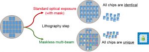
Figure 2. Wafer exposure strategy
• With repeated identical chips on optical scanner
• With diversified unique chips with Mapper FLX-1200 tool
The multibeam technology’s suitability for insertion in existing silicon-chip manufacturing has been demonstrated directly on product wafers manufactured in a conventional IC fab[1]. This first customer demo involved wafers from a mature industrial CMOS N40 flow at via-3 level with copper-based interconnects (BEOL). The product wafers were exposed on the FLX-1200 multi‑beam tool at 5kV by printing the metrology blocks located in the corner of the frame and the N40 logic cell inside the field with via features designed at 63nm. Each block size represented an area 3x3mm² (Figure 3). Leti has developed a lithographic stack containing standard industrial materials, as used today for optical scanners. The e-beam resists are chemically amplified type resists. The lithographic performances and etch transfer results were fine-tuned on customer wafers to fit the N40 specification targets in terms of CD control, CD uniformity and pattern fidelity.
Specific circuit structures on demand
The fruitful partnership between Leti and Mapper produced a unique competence-and-technical combination for data preparation, proximity-effect corrections, tool monitoring, metrology and etch-transfer processes. Matching strategy with standard optical scanner is now operational and qualified thanks to the optical-alignment system installed inside the FLX-1200 platform, which enables mix-and-match operations with conventional optical lithography.
The collaboration also developed a complete integration process flow. Final technical results are compliant with industrial specifications for the N40 dual-damascene process flow. This achievement confirms that Mapper’s technology can be qualified for IC CMOS 40nm-node logic, including specific process steps (Figure 3):
- Wafer clamping on silicon wafer, including metallic deposit layers
- Customer design transfer on the machine without execution errors
- Reading alignment marks created with standard optical scanner
- Alignment on the buried layer and exposing the layout of real products.
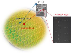
Figure 3. Pattering demonstration on first customer 300 mm wafer exposed
with FLX-1200 multi beam tool at 5kV (Via layer node 40nm CMOS)
This successful demo is promising for Mapper, as it demonstrates compliance with the CMOS manufacturing standard. It also shows the ability to write on-demand specific circuit structures at any desired location, answering the basic expectation of any designer to realize unique and secured CMOS chips.
This via patterning integration on production wafers shows the latest achievements obtained on the Mapper FLX-1200 platform, while demonstrating its compatibility with standard optical lithography and its capability to be transparently inserted into standard CMOS integration flow. This technology maturity, therefore, moves from the level of proof of concept to the pre-production level. To further the platform’s maturity, Mapper and Leti will pursue intensifying the tool hardening. They will also extend the overall demonstration program to highlight and value the capability of this technology to fully meet industry needs and expectations. This activity of cyber-security, one of CEA Tech’s key expertise areas, is actively developed, as it represents a clear technology path for the manufacturing of tomorrow’s devices. Furthermore, the FLX-1200 platform installed in Leti’s silicon pilot line is also now accessible for private customer patterning demonstrations (please contact authors: laurent.pain@cea.fr, isabelle.servin@cea.fr)


