
Introduction
HDMI is a wired transmission standard for uncompressed video signals between consumer home electronics equipment.
Uncompressed video requires a high data rate. For example, an HDTV picture displays 1920 * 1080 = 2 073 600 pixels, with each pixel consisting of 3 color values (red, green and blue) with 8-bit quantization. For historical reasons, a synchronization frame with free data ranges (e.g. for audio) is added along with additional bits for transmission coding. An increase in the quantization (“deep color”) is also possible, which naturally requires an increase in the data rate.
In total, HDMI transmission requires a data rate range of
3 * 250 Mbit/s up to 3 * 3.30 Gbit/s for all conventional aspect ratios and refresh rates. This range is specified by HDMI 1.4b.
For UHDTV (4k) with refresh rates of 50 Hz or 60 Hz, the data rate was extended in HDMI 2.0 to 3 * 5.94 Gbit/s. The factor 3 is used here because HDMI is equipped with 3 data lines.
Serial data transmission in accordance with the HDMI standard
Data on HDMI cables is transmitted serially on one wire pair using current mode logic. In other words, the transmitter contains a current sink that is switched so that it is out of phase with one or the other wire, depending on the logic information. The receiver terminates the wires with 50 ohm to +3.3 volt and uses a differential amplifier to access the logic information.
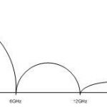
The spectrum of the HDMI data signal corresponds to that of digital NRZ signals and is made up primarily of signal components up to the bit rate and additional components up to 2 and 3 times the bit rate. For signal analysis at 5.94 Gbit/s, this translates into a required measurement bandwidth of up to 18 GHz.
These high bandwidth requirements apply not only to the test instrument, but also to the plug connector and the cabling to the test instrument.
-

- Fig. 1: Spectrum for a 6G TMDS in line with HDMI 2.0
-
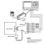
- Fig. 2: Example test setup for measuring the TMDS eye diagram (source: HDMI 1.4 specification)
-
- Fig. 3: Specification for measurement of the TMDS eye diagram (source: HDMI 1.4 specification)
-
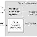
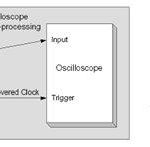
- Fig. 4: The clock recovery unit
Compliance tests
To ensure connectivity of devices from a wide variety of manufacturers, the HDMI Forum has prepared the Compliance Test Specification (CTS). This specification assists in assessing the characteristics of HDMI components or consumer electronics equipment. Manufacturers are authorized to use the HDMI logo for devices that pass these tests. A portion of the tests is based on the electrical characteristics of HDMI signal sources.
This document specifically addresses these electrical tests for HDMI sources, which alone represent an enormous investment in test equipment.
Typical test equipment required for measuring the signal quality of an HDMI source includes a real-time oscilloscope (RT scope) connected to the HDMI source under test via an HDMI test point access adapter (Fig. 2).
However, the serial data transmission characteristics for HDMI described above are extremely demanding on the RT scope. A sampling rate of 40 Gsample/s and an analog bandwidth of > 12.5 GHz for HDMI 2.0 signals or a minimum of 20 Gsample/s and 8 GHz bandwidth for HDMI 1.4b are the basic requirements.
Some of the tests are defined as time difference and voltage measurements at specific trigger points, while other measurement values are calculated from statistical information (eye diagram). The test specification precisely describes how to perform the tests using RT scopes. A less time-consuming and less costly alternative is eye diagram measurement using subsampling. Signal parameters such as amplitude and time are determined exclusively from the measured eye diagram, without the option of triggering on specific bit sequences. The measurement principle is explained below.
-
- Fig. 5: Principle behind subsampling
-
- Fig. 6: Block diagram of the HDMI test point access adapter
-
- Fig. 7: Block diagram of the base module
-
- Fig. 2 1: TMDS clock jitter measurement
Principle behind the data eye diagram measurement
Subsampling The intent of the data eye diagram measurement is to ensure that an HDMI sink receives data from an HDMI source without errors. This is done by means of an eye diagram measurement. The eye diagram can be used to assess the signal quality and to determine possible transmission errors. The HDMI CTS defines how the measurement has to be carried out, which is shown in Fig. 3.
To display the eye diagram, the clock recovery unit (CRU) is used to recover the data clock from the TMDS clock (see Fig. 4). The recovered clock is used to trigger the oscilloscope, which lays all waveforms over each other. The CRU follows the TMDS clock to a certain extent. The CRU transfer function is specified in detail in the HDMI standard.
The HDMI standard assumes that the measurement is performed using a real-time oscilloscope (RT scope). With a RT scope, the CRU as well as the formation of the eye diagram are realized in software. Measurements of HDMI 2 signals require an analog bandwidth of >12.5 GHz. This equates to sampling rates of ~40 Gsample/s, making these instruments very large and expensive.
The Rohde & Schwarz VT-B2380 TMDS time domain analyzer solution, on the other hand, presents an alternative approach to the RT scope: subsampling. Subsampling makes use of the fact that the data is recurring and the statistical characteristics remaining fairly constant over the duration of the measurement. Advantages of subsampling include decreased hardware complexity while retaining a high analog bandwidth of >12.5 GHz, good integrability, low thermal losses and a significant cost advantage.
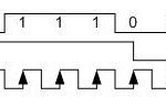
The principle behind subsampling is shown in Fig. 5. The applied analog signal TMDS_Dx is to undergo subsampling. The clock designated as CRU_x corresponds to the clock CRU, but can also be additionally varied in phase φ. During subsampling, the phase is varied in steps Δφ and a certain number of samples is taken for each phase value. (CRU_1, CRU_2,…) The result is a scatter plot of samples that is clearly associated with one phase value.
The figure illustrates the process for CRU_3. During the measurement, the phase φ remains constant. A sample is taken at each rising edge of CRU_3 (five samples in total in this example) and then drawn into the reconstructed waveform TMDS_Dx~, indicated by arrows. As can be seen here, samples 1 and 3 coincide, as do samples 2 and 5. As soon as the desired number of samples has been taken, the phase is increased by one step Δφ and the process repeated. (CRU_4, etc.)
In practice, the phase steps Δφ are minimized such that a continuous impression is generated and the signal waveform is reconstructed cleanly.
In contrast to the RT scope, for subsampling the CRU must be implemented in hardware. A later software calculation is no longer possible because the Nyquist criterion is intentionally violated.
The intentional violation of the Nyquist criterion means that subsequent signal processing of the eye diagram is possible only to a very limited extent. If, for example, the input data is unknown (which is the case with HDMI), a given frequency response cannot be calculated in the eye diagram.
-
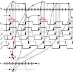
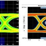
- Fig. 8: Media player with fTMDS_CLK = 148.5 MHz
-
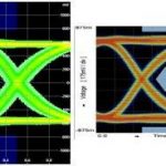
- Fig. 11: Receiver with fTMDS_CLK = 74.25 MHz
-
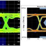
- Fig. 10: Media player with fTMDS_CLK = 296.7 MHz
-
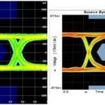
- Fig. 9: HDMI generator with fTMDS_CLK = 297.0 MHz
R&S®VT-B2380 TMDS time domain analyzer
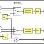
The TMDS time domain analyzer (TDA) is a sampling oscilloscope (an oscilloscope that uses the subsampling principle) that has been optimized for HDMI requirements. It consists of an HDMI test point access adapter (TPA) and a base module.
The portion of the HDMI TPA adapter block diagram relevant to the eye diagram measurement is shown in Fig. 6. For the eye measurement, the HDMI TPA adapter is connected to an HDMI source. The adapter communicates with the HDMI source and brings it into a state where data is output to the TMDS-Dx differential pairs. The HDMI TPA adapter automatically selects one of the four TMDS differential pairs and connects it via the cable to the TDA module, saving the user from having to move the connection. The equalizer and amplifier compensate for the cable frequency response. The TMDS wires must be terminated appropriately for both AC and DC. The probe ensures the correct termination.
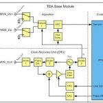
The block diagram for the TDA module is shown in Fig. 7. The differential input signal TMDS_Dx+/– from the HDMI TPA adapter passes over an optional termination directly to a fast sampler with >15 GHz analog bandwidth. The sampler uses sample frequency fS to obtain the signal value and holds it until the downstream ADC has converted the value.
The HDMI-specific portion of the TDA module consists mainly of the clock recovery unit (CRU). The clock TMDS_CLK with frequency fTMDS_CLK is in a fixed ratio to the data TMDS_Dx with bit rate fTDMS_DATA. The ratio is different for HDMI 1.X and HDMI 2. The allowed frequencies and bit rates are summarized in Table 1. The ratio between the bit rate fTMDS_DATA and the clock fTMDS_CLK is also known as the serialization factor.
As seen in Table 1, the CRU must work with a wide range of possible input frequencies. The HDMI specification precisely specifies the transfer function for the CRU. According to the standard, a PLL with the following transfer function is required:
H(jω)=1/(1+j ω/ω0)
,ω0=2π∙4.0MHz
Equation 2 1: Jitter Transfer Function for ideal recovery clock definition
The clock recovery in the TDA module consists of a PLL that includes the following blocks: divider 1 to 3, phase detector, loop filter and VCO. The PLL uses the input clock fTMDS_CLK to derive the sample frequency fS. The loop filter approximates the transfer function (see formula) as best possible.
The output signal of the phase detector is proportional to the phase between input clock fTMDS_CLK and sample frequency fS. By adding a phase offset Δφ (see Fig. 7) to the output signal of the phase detector, the phase is systematically changed, thereby reconstructing the waveform TMDS_Dx~ step by step as shown in Fig. 5.
The overall module is controlled via the instrument firmware in conjunction with an FPGA.
R&S®VT-B2380 TMDS clock jitter measurement
HDMI defines TMDS clock jitter as the maximum deviation of the TMDS clock signal phase relative to an ideally recovered reference clock. This ideal reference clock can be derived from the clock signal via the clock recovery unit (CRU).
The extent of jitter present in the measured value mainly depends on the measurement time and the CRU’s transfer function. The measurement time is determined by the oscilloscope’s memory depth and the selected sample frequency. An ideal transfer function has been specified for the CRU (see Equation 2 1).
As explained above, the CRU in the R&S®VT-B2380 is implemented in hardware, not software. Its transfer function only approximates that of an ideal CRU. This means that, depending on the jitter frequency, there can be deviations in the measurement results compared with a digital oscilloscope. These deviations constitute a measurement uncertainty (see Appendix A).
In addition, the jitter measurement accuracy data in the Appendix takes into account the fact that jitter measurements in the R&S®VT-B2380 are always performed without an equalizer. An equalizer should be used for clock rates higher than 165 MHz in order to minimize the effect of noise on the jitter measurement.
This measurement uncertainty must be taken into consideration when assessing whether the DUT complies with the specification.
Examples
In this section, different HDMI sources are measured with the R&S TMDS time domain analyzer (TDA) and a real-time oscilloscope (RT scope) and the results are compared.
Eye diagram
The results from the TDA are shown below on the left and those from the RT scope on the right.
The measurement results in Fig. 8 and Fig. 9 correlate very well. The amplifiers in the HDMI TPA adapter only negligibly increase the noise in comparison to the RT scope, which does not use amplifiers.
The waveforms in Fig. 10 deviate somewhat from one another. This could be caused by slightly differing termination impedances on the two test instruments.
The waveforms in Fig. 11 deviate significantly. This effect is caused by a strongly fluctuating DC component in the HDMI signal. Because part of the signal is AC-coupled within the HDMI TPA, a varying DC component vertically shifts the reconstructed waveform. This shift cannot be eliminated after the measurement.
It is a characteristic of the transition minimized differential signal (TMDS), although it does not negatively affect differential receivers.
Note: Because this DC component is not optimal for data transmission at high bit rates, HDMI 2.0 introduced scrambling for 6G signals.
Conclusion
Measurement of the electrical characteristics of an HDMI signal using conventional test equipment is both cost-intensive and time-consuming. The process described here permits the implementation of a compact and economical solution that provides information about the physical quality of a TMDS source quickly and without complications.
The implementation using the R&S VT-B2380 TMDS time domain analyzer is additionally combined with a compact TPA adapter. This minimizes the required cabling and eliminates the need to move cables during the measurement. In addition, all required components, including the BIAS-T and EDID source, are already integrated and do not need to be provided externally.
The TMDS measurement offered by the solution additionally covers measurements on the control and communications bus, further reducing the number of required instruments.
The user-friendly R&S VT-B2380 TMDS time domain analyzer guides the user through the measurements so that in-depth knowledge of the individual HDMI-specific measurements is not absolutely necessary. Even the application of the specific EDID to the DUT is performed automatically.
The subsampling measurement principle described here deviates from the process described in the HDMI CTS for determining the electrical quality of HDMI sources. As a result, it is not possible to trigger on data words and to acquire specific signal sequences. However, the procedure does make it possible to assess the quality of an HDMI output in a good approximation of the HDMI CTS requirements.


