NXP Semiconductors N.V. (NASDAQ:NXPI) is first to market with a new applications processor design that leverages Fully Depleted Silicon On Insulator (FD-SOI) technology to offer the industry’s lowest power consuming general-purpose processor. Coupling FD-SOI with the company’s multiple fully independent domain architecture, NXP’s innovative design delivers a deep sleep suspend power consumption of 15 uW or less, 17 times less in comparison to previous low power i.MX 7 devices, while the dynamic power efficiency is improved by 50 percent on the real time domain. This new design based on FD-SOI’s lower voltage capability enables rich user experience through extremely power-efficient graphics acceleration, a fundamental requirement in many of today’s consumer and industrial battery-operated devices that incorporate robust graphic interfaces. Further enablement includes rich Linux or Android ecosystem with the real-time capability supported by FreeRTOS.
“Power consumption is at the heart of every decision we made for our new applications processor design, which now makes it possible to achieve stunning visual displays and ultra-low power standby modes in a single processor,” said Joe Yu, vice president of low power MPUs at NXP. “From the selection of the FD-SOI process and dual GPU architecture, to the heterogeneous processor architecture with independent power domains, every aspect of our new processor design is aimed at providing the best performance and user experience with unprecedented energy efficiency.”
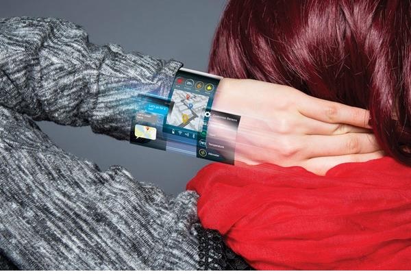
The design’s extreme low leakage and operating voltage (Vdd) scalability is attained through reverse and forward body biasing (RBB/FBB) of the transistors and its smart power system architecture. This high performance, low power solution is optimized for customers developing IoT, home control, wearables and other applications that spend a significant amount of time in standby mode with short bursts of performance-intense activity that require exceptional graphics processing.
NXP’s unique FD-SOI design enables:
- Large dynamic gate and body biasing voltage (Vbb) range
- Domain and subsystem optimization with custom standard cell library with mixed voltages
- Low quiescent current (Iq) bias generators
- Enhanced ADC performance with unique FD-SOI attributes
- Fail Safe I/O for simplified low power system design
“We are excited that NXP is the first to bring the benefits of FD-SOI (28FDS) technology to the general purpose market,” said Ryan Lee, VP of the Foundry Marketing Team at Samsung Electronics. “28FDS technology will satisfy a growing and critical need for ultra low power designs that require power-performance at very low voltages. We plan to evolve 28FDS technology to a differentiated low-power single platform by implementing RF and embedded Non-Volatile Memory (eNVM) solution for our customers’ success.”
NXP’s processor design enables robust low power graphics for the IoT and Wearable markets through two graphic processor units (GPU) from Vivante–the GC7000 NanoUltra 3D GPU with a low power single shader, and the GC320 Composition Processing Core (CPC) for 2D graphics. The 3D GPU plays a critical role in enabling rich 3D based user interfaces, while the CPC can accelerate both rich 3D and simpler 2D user interfaces. Processors based on the combination of the two GPUs enable efficient display systems which offload and significantly reduce system resources, in turn providing rich user interfaces at low power levels to extend the battery life of devices.
“Our 3D GPU is a result of a joint collaboration between Vivante and NXP to deliver industry-leading 3D capabilities with the lowest power consumption,” said Wei-Jin Dai CEO at Vivante Corporation and Chief Strategy Officer and GM of IP Division at Verisilicon. “The power savings from using the right GPU in an ultra low power processor is one of the major attributes and advantages of the architecture.”
Availability
The i.MX 7ULP applications processor family is currently sampling to select customers. Broader availability of pre-production samples is scheduled for Q3 2017.
See NXP Technologies in Action at Embedded World 2017 in Nuremberg, Germany
Visit NXP during Embedded World in Hall 4A – 220 at the Exhibition Centre Nuremberg. See the new i.MX 7ULP applications processor in action and interact with other innovative demonstrations for embedded solutions enabling the IoT from smart cars to smart industry.