

Introduction
The growing complexity of board-level designs has begun to strain the capabilities of today’s hardware/power management architectures. While any one of the four most commonly used management architectures can be used to support these complex designs, they each require different sets of compromises and design trade-offs in terms of scalability, design effort or cost.
Recently, a fifth board management architecture has emerged which provides the best possible performance, safety and flexibility while requiring far less design effort and implementation cost. This article will explore this new architecture, primarily with a focus on the Power Management functions it provides.
-

- Figure 1. Smart car systems

-
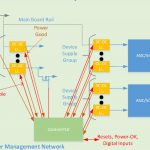
- Power Architecture #1: Power Management & Housekeeping by Control PLD —– Fig.2: A Hardware Management system implemented using a Control PLD to perform Power Management and Housekeeping.
-
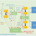
- Power Architecture #2: Power Management using Power Manager ICs with Housekeeping by Control PLD —– Fig.3: A Hardware Management system implemented using Power Manager ICs and a Control PLD.
Overview
A circuit board is typically divided into 2 functional blocks (Figure 1), the Payload Management section and the Hardware Management section. In most boards, 80% – 90% of the circuit board is typically devoted to “payload” functionality (data/control plane elements and/or processors). The remaining 10%-20% of board space is occupied by the circuitry which performs hardware-level monitoring/control or housekeeping functions.
Unfortunately, most existing Hardware Management solutions have difficulty scaling to address the growing complexity of modern Payload Elements. For example, although the Hardware Management section typically occupies only 10% – 20% of the board, its design/debug effort can consume a much larger percentage the overall development time (30% – 40%). Likewise, the Hardware Manager often consumes a disproportionate share of the overall Bill of Materials (BOM) cost.
Recently however, a new distributed architecture has been developed which is much more scalable and can be implemented at a much lower BOM cost. In order to better understand the advantages a distributed architecture offers, we’ll look at how Power Management is implemented in four of the most commonly used Hardware Management architectures (illustrated in Figures 2-5) before taking a deep dive into the distributed architecture (illustrated in Figure 7).
-
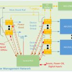
- Power Architecture #3: Housekeeping using Control PLD with Microcontroller-based Power Management through a PMBus — Fig.4: A Hardware Management system implemented using a Control PLD and an MCU
-
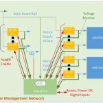
- Power Architecture #4: Power Management and Housekeeping using a Control PLD with on-chip ADC —- Fig.5: A Hardware Management system implemented using a Control PLD with an on-chip ADC
-
- Fig.6: The L-ASC10 remote sensing element.
-
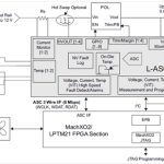
- Power Architecture #5: Power Management and Housekeeping performed by a Control PLD with L-ASC10 (ASC) providing Distributed Voltage Sensing & control —- Fig.7: – A Hardware Management system implemented using a distributed architecture

A comparison of Control PLD based power management architectures
In the following analysis, we’ll compare how these supplies are managed by each of four commonly used architectures (illustrated in Figures 2-5).
In this architecture, the power management functions are added to the on-board control PLD. The control PLD monitors the “Power Good” signals of the input supply and each DC-DC converter (Fig.2). The sequencing algorithm implemented in a Control PLD generates the sequence of “Enable” signals needed to turn on the power to the payloads without causing damage or logical errors.
The Control PLD also generates logical signals such as resets and power good to ensure that the payload devices can begin operation during power up or terminate their operations during power down. It is also responsible for generating a sequence to safely disable the supplies during power-down or when a fault is detected. PLDs can easily support Event-Based solutions which provide different responses to different combinations of faults.
For this class of designs, all the power sequencing, protection and control functionality is implemented within the Control PLD, typically using VHDL or Verilog.
Pros:
• Low cost
• Straightforward architecture enables the Control PLD’s sequencing logic to be easily scaled to accommodate new applications.
• Designs can be implemented using a single design environment (typically VERILOG).
• Event-based architecture can respond to individual fault modes in a flexible manner.
Cons:
• Since each supply requires two signal paths, larger, more complex designs begin to suffer from high Control PLD I/O count and board congestion.
• Reduced reliability because the Power Good fault detection is inaccurate (typically 8% to 20% error) and cannot monitor trends in supply voltage.
• Adding Telemetry (monitoring the actual supply voltages instead of the Power Good signal) requires adding an A/D converter, increases cost & complexity to the board.
• Requires a board-level engineer (with digital expertise) to implement, someone who, in many cases, is not be a power supply expert.
In this split-function architecture, a Power Manager IC is responsible for monitoring and sequencing the board’s DC-DC converters (Fig.3). Because it directly monitors the supply’s voltage the Power Monitor can also perform trimming and margining. The Control PLD uses the supplies’ Power Good status lines to generate the necessary control, status and housekeeping signals.
For these designs, the Power Manager functionality is typically defined using GUI-based configuration tools while the Control PLD logic is defined using VHDL or Verilog.
Pros:
• Lower Control PLD I/O count because the Enable function is handled by the Power Manager.
• Lower board congestion means a simpler layout and fewer board layers.
• By directly monitoring the supply voltages, the Power Monitor IC can get a more accurate picture of overall system health and enable higher system reliability.
Cons:
• Power manager ICs increase BOM cost – especially if multiple devices are required.
• This architecture can provide Event-Based response but it adds to design complexity if more than one Power Manager is employed.
• Scaling sequencing to more complex designs can be difficult – especially if it involves partitioning functionality across multiple Power Manager ICs.
• Since the design process is spread across multiple tools (GUI + VHDL/Verilog), it may require multiple engineers and increase design risk.
Figure 4 illustrates an architecture which uses a microcontroller (MCU) to perform the sequencing of digitally-controlled point of load (DPOL) supplies. The MCU manages the DPOLs using the Power Management Bus (PMBus), a two wire communications protocol based on the I²C bus. This leaves the Control PLD responsible for supporting the board’s housekeeping functions as well as controlling any point-of-load DC-DC converters which have an analog control interface (APOLs).
To simplify the software design, most MCU-driven power management designs employ Time-Based sequencing schemes which issue a single fixed sequence of disable signals to power down the board when a normal turn-off is requested or when a fault condition is detected.
Another potential drawback of software-based power management is that it is slower to respond to fault conditions (typically 10-15 milliseconds versus the microsecond-scale response of a Control PLD). If some fault conditions require a faster response (or Event-Based sequencing), a second layer of protection may be added using the Control PLD.
Implementing software-based Power Management requires both, software for the MCU and a Control PLD design, written in either VHDL or Verilog.
Pros:
• Designs are easily scalable (for time-based sequencing only).
• Abundant software development tools make MCU-based solutions faster and easier to debug.
• Designs can be quickly modified using firmware updates.
• Simpler PCB designs – routing congestion reduced around DPOLs
Cons:
• More expensive BOM
• Difficult to scale if Event Based sequencing is required.
• Multiple design tools required (Verilog/VHDL + Software)
• Mix of APOL & DPOL requires a hybrid control solution which has several drawbacks:
o It cannot be simulated easily.
o Hardware management functions can only be tested in a prototype board environment.
o Complexity increases system debug times.
In order to overcome issues with inaccurate Power-Good signals, it’s possible to monitor the board’s supply voltages using a Control PLD that’s equipped with an on-chip digital converter (ADC). In this architecture, the Control PLD implements the power management functions using an on-chip soft/hard processor core while housekeeping functions are implemented in hard logic (Fig.4).
For these types of designs, the designer usually develops the Power Management function in software and the other housekeeping functions using VHDL/ Verilog.
Pros:
• The solution can be easily scaled or adapted for other designs.
• Combining Power Management and housekeeping functions reduces design time.
• This architecture can provide voltage telemetry to a remote system manager.
Cons:
• Requires a larger CPLD with higher density and I/O pin count.
• Complex CPLD increases solution cost.
• Routing low-voltage analog telemetry to a single location increases circuit board congestion.
• Forces a digital engineer to implement both power management function as well as digital control functions.
Introducing a Distributed Power Management Architecture
A Distributed Power Management architecture eliminates the need for many of these trade-offs through the use of a low-cost Analog Sense and Control (ASC) power management element. These devices enable the implementation of complete hardware management functions (Power and temperature management as well as control path and housekeeping functions are collectively referred to as hardware management function).
Lattice Semiconductor’s L-ASC10, is a Hardware Management (Power, Thermal, and Control Plane Management) Expander. It can be used in conjunction with Control PLDs such as Lattice’s low-cost MachXO2 series to implement the Hardware Management function in a circuit board. Figure 6 illustrates how the Hardware Management functionality would be divided up between the L-ASC10 and its companion MachXO2 Control PLD.
Each of the analog sense channels is monitored through two independently programmable comparators to support both high/low and in-bounds/out-of-bounds (window-compare) monitor functions. Communication between the ASC and the Control PLD is accomplished through a single 3-wire serial bus (Tx/Rx/Ck).
As we’ll see in the following scenario, using a single serial bus to monitor and control multiple power supplies greatly reduces both the number of I/O pins required for the PLD.
In a distributed Hardware Management architecture, the Control PLD uses several external ASC devices to monitor supply voltages. The Control PLD also transmits Enable/Disable commands to the DC-DC supplies and performs other housekeeping functions.
Both Power Management & housekeeping functions can be implemented using a GUI tool, VHDL/Verilog, or a combination of both.
PROs:
• Common 3-wire bus requires the minimum number of Control PLD I/O pins.
• Simplified PCB traces create the least board congestion.
• The entire system can be implemented in a single design environment (GUI or VHDL/Verilog)
• Distributed architecture is highly scalable.
• Reduced solution cost because the voltage, current and temperature monitoring functions are integrated within the ASC.
• Reduced design time as Power Management and housekeeping functions are together.
• Dramatically reduce board debug time using Lattice’s standard power debug utilities.
Conclusions
As the complexity of board-level systems has grown, Hardware Management systems have begun to consume a disproportionate share of design effort and BOM costs. Now, a distributed Hardware Management architecture is available which connects a control PLD to low-cost sensing elements through a 3-wire serial link. In addition to reducing design complexity, board space requirements and BOM costs, this architecture may be implemented with a wide variety of tools, commonly used by power and digital designers.
For Further Reading:
“Revolutionary Hardware management Solutions”, A Lattice Semiconductor White Paper, April 2015 https://www.latticesemi.com/view_document?document_id=51004
L-ASC10 Data Sheet – https://www.latticesemi.com/view_document?document_id=50120
“Adding Scalable Power and Thermal Management to MachXO using L-ASC10” A Lattice Application Note https://www.latticesemi.com/view_document?document_id=50995


