


Leti, an institute of CEA Tech, presented two papers at IEDM 2016 today that demonstrate its ability to provide industry with all the elements required for building a competitive 5-nm node with nanowire architectures.
Nanowire architectures are seen as the best candidates for that node, and Leti is addressing some of its biggest challenges, such as of performance and parasitic capacitances. Its results suggest that strain can be introduced into stacked nanowire and that parasitic capacitances can be reduced thanks to inner spacer integration.
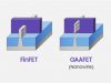
The paper, “Vertically Stacked-Nanowires MOSFETs in a Replacement Metal Gate Process with Inner Spacer and SiGe Source/Drain”, is the first demonstration of functional devices with SiGe source and drain to induce strain in the channel to boost performance, and inner spacer to reduce parasitic capacitances. Both building blocks are required for the 5-nm node. This MOSFET architecture extends the scaling limits of CMOS technology, and is also seen as a possible extension to FinFET.
Leti, at IEDM 2008, was among the world’s first organizations to report stacked nanowire and nanosheet results.
The second paper, “NSP: Physical Compact Model for Stacked-planar and Vertical Gate-All-Around MOSFETs”, presents a predictive and physical compact model for nanowire and nanosheet gate-all-around MOSFETs.
“This is the first compact model, or SPICE model, that can simulate stacked nanowire and nanosheet devices with various geometries,” said Olivier Faynot, Leti’s microelectronics section manager and a co-author of both papers. “It also enables the simulation of vertical nanowire, which is one of the key achievements of this model.”
The paper presents a physically based SPICE model for stacked nanowires that can enable circuit designers to accurately project their existing circuits into the 5-nm node, and investigate novel designs.