

Overview
This application note demonstrates a simulation-based methodology for broadband power amplifier (PA) design using load-line, load-pull, and real-frequency synthesis techniques. The design highlighted in this application note is a Class F amplifier created using the Qorvo 30 W gallium nitride (GaN) high electron mobility transistor (HEMT) T2G6003028-FL. Goals for this design included a minimum output power of 25 W, bandwidth of 1.8 – 2.2 GHz, and maximum power-added efficiency (PAE). The design procedure was performed using the Modelithics GaN HEMT nonlinear model for the Qorvo transistor in conjunction with NI AWR Design Environment™, inclusive of Microwave Office circuit design software, Modelithics Microwave Global Models, and the AMPSA Amplifier Design Wizard (ADW).
-

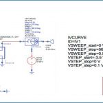
- Figure 1: Initial load-line analysis and harmonic impedance tuning. Left side is the schematic to bias and stabilize transistor and right is the IV curve simulation schematic
-
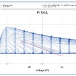
- Figure 2: Final results of tuning with IV curves with dynamic load line superimposed
-
- Figure 3: Smith chart view of the fundamental and harmonic impedances of the output tuner

-
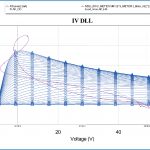
- Figure 4: Final dynamic load-line after harmonic impedance tuning
Design Overview
The design for this PA began with measurements of the voltage and current at the drain-source intrinsic current generator within Microwave Office. The near optimum load line, terminating impedances at the fundamental frequency, and impedances at harmonic frequencies for a single-drive frequency were located for the required mode of operation. The impedance regions were then extracted using load-pull simulations. Using ADW with Microwave Office software, the real-frequency synthesis of the matching networks was quickly realized simultaneously for the fundamental and harmonic impedances across a wide bandwidth. These fully laid-out matching networks were then exported to Microwave Office software for the remainder of the design optimization, nonlinear analysis, and electromagnetic (EM) simulation.
Design Process
To begin the design process, a schematic was created to bias and stabilize the transistor. Once the conditions required for stability and biasing were established, the initial load-line analysis and harmonic-impedance tuning could be performed, as shown in Figure 1.
-
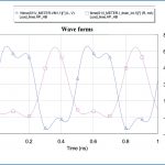
- Figure 5: Intrinsic voltage and current waveforms after harmonic impedance tuning
-
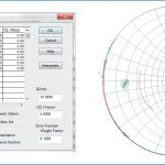
- Figure 7: The load-pull contours of the fundamental frequency for maximum power (blue) and drain efficiency (magenta) have been plotted in the same Smith chart. The green circle defines the region of mutually acceptable power and efficiency
-
- Figure 6: Load-pull simulation schematic

-
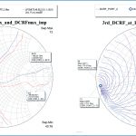
- Figure 8: Left – Plot of load-pull contours for the second harmonic frequency at the fundamental impedances for maximum power and drain efficiency. The acceptable region is below the drawn line. Right – Plot of load-pull contours for the third harmonic frequency at the fundamental impedances for maximum power and drain efficiency. The acceptable region is above the drawn line
Initial Load-Line and Harmonic Impedance Tuning
First, a line was drawn on top of the IV curves to approximate the near-optimum load line for the fundamental frequency (the maximum swing of the RF voltage and current before hard clipping occurs). A dynamic load line was defined using meters located within the model to monitor the intrinsic drain voltage and current and superimposed on the IV curves by the IV dynamic load line (DLL) measurement. It was then tuned to be a straight line and parallel to the drawn line. The tuning at a chosen frequency was performed by tuning the magnitude and phase of the output tuner impedances. At this stage, the harmonic balance (HB) simulation was limited to just a single harmonic – the fundamental frequency. Additionally, the harmonic impedances of the output tuner and all the impedances of the input tuner were set to 50 ohms. The final results of this load-line tuning can be seen in Figure 2.
Once the impedance of the fundamental frequency was determined, the second and the third harmonic impedances presented to the intrinsic drain were tuned according to the desired mode of operation. In the case of this application note, Class-F operation was desired, meaning that the second harmonic impedance was tuned to a short circuit and the third harmonic impedance was tuned to an open circuit, as shown in Figure 3.
The fundamental impedance of the input tuner was then set to be a conjugate match to the S11 of the transistor and stability / bias network. This would provide the best match, and, therefore, maximum gain. The harmonic impedances of the input tuner were set to 50 ohms.
Once all of the impedances were tuned, a final harmonic balance simulation (using three harmonics) was performed to confirm the design was in the desired mode of operation. Figures 4 and 5 show the classic shapes of a Class-F mode design.
-
- Figure 9: Left – Examples of the termination definition facilities in ADW. Right – Smith chart view of desired termination impedances (red, grey, pink, and blue) versus achieved impedances (green)
-
- Figure 10: Left – Initial hybrid microstrip / lumped-element output-matching network created in ADW. Right – Final output matching network after decoupling elements, optimization, and layout manipulation is complete
-
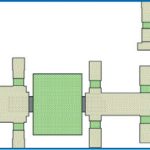
- Figure 11: Final layout for the Class-F amplifier design
-
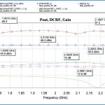
- Figure 12: Final simulated performance for the Class-F amplifier design
Load-Pull Impedance Extraction
With the previously defined input and output impedances, load-pull simulations were performed to produce contours, first for maximum power (Pmax) and then for maximum drain efficiency (DCRF). The same schematic was used for the load-pull simulations as for the initial tuning, except for the addition of an XDB control element (Figure 6). This provided contours that were not only at a constant power and efficiency, but also at a constant gain compression.
Notice that the schematic is identical to that of Figure 1, however, the input and output impedances have been updated and the XDB component has been added.
In Figure 7 the contours at the fundamental frequency for both maximum power and efficiency have been superimposed in order to define a region of compromise for mutually acceptable power and efficiency. In this case, an output power 1 dB below the maximum and an efficiency five percent below the maximum was chosen. In the plot shown in Figure 7, a circle defining this region was placed by using an equation to define the acceptable area of the fundamental frequency impedance for the synthesis of the relatively broadband output network.
In the next step, load-pull simulations for second and third harmonic frequencies were performed at the two impedances that provided the maximum power and maximum efficiency in the load-pull simulation of the fundamental frequency. The results for both load-pull simulations at the second and third harmonic can be seen in Figure 8. For the simulation at the second harmonic frequency, the optimum maximum efficiency in both cases was the same and the contours were essentially the same. A line was drawn to bound the area with acceptable performance. In this case, the acceptable region was below the line. For the simulation at the third harmonic frequency, the optimum maximum efficiency was again the same in both cases, however, the contours differed somewhat. Fortunately, the effect of varying the third harmonic impedance was small and an acceptable region was easily defined above the drawn line.
The described impedance extraction process was performed for a few frequencies across the desired bandwidth. In the case of this application note, simulations for 1.8 GHz, 2 GHz, and 2.2 GHz were sufficient. It is important to note that this was a streamlined method of extracting the fundamental and harmonic impedances that relied on access to the voltage and current across the intrinsic generator. Access to the intrinsic device nodes enabled a near optimum tuning of the fundamental load line (impedance) and allowed for fixing the harmonics impedances for a particular mode of operation at the outset of the design flow. This capability, along with model availability, greatly sped up the design process by reducing iterative tuning between fundamental and harmonic load impedances.
If the transistor model was a black box or the intrinsic access was not used, the load-pull impedance extractions would need to be performed for far more iterations. First, load pull for the fundamental frequency would have to be performed with the harmonics set to 50 ohms. Then, the load pull would have to be performed for harmonic loads and then with the newly found harmonic impedances. For the highest performance, load-pull analysis/optimization at the fundamental frequency would again need to be repeated. More iteration would be needed for the harmonics, and at that point one might want to stop the iterations. The issue with this approach, other than the number of iterations required, is the uncertainty that optimum loads have actually been defined, and nothing would be known of mode of operation.
-
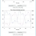
- Figure 13: Simulated intrinsic device channel voltage and current wave forms at 1.8 GHz (top), 2 GHz (center), and 2.2 GHz (bottom).
-
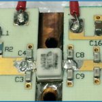
- Figure 14: Assembled Class-F amplifier design
-
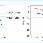
- Figure 15: Simulated versus measured output power (red), PAE (blue), and S21 (green). Lines show simulated performance; symbols show measured data

-
- Figure 16: Simulated versus measured small signal S-Parameters
Matching Network Synthesis
Once all impedances were determined, ADW was used to synthesize the broadband matching networks. The required fundamental and harmonics impedance areas across the desired bandwidth were defined in the corresponding facilities of ADW, shown in Figure 9. The fundamental impedance areas for each frequency are circles on the Smith chart. The harmonic impedance areas are sections of the Smith chart.
Based on the impedances input into ADW, an initial hybrid microstrip / lumped-component output-matching network was synthesized (left image in Figure 10). The initial design was then exported into ADW’s analysis facility for the addition of all decoupling components, optimization, and layout manipulation. The final output-matching network design can be seen on the right in Figure 10. The same process was performed for the input matching network and both designs were exported to Microwave Office software to finalize the design.
-
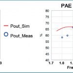
- Figure 17: Simulated versus measured output power (left) and PAE (right)
-
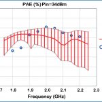
- Figure 18: Results of a preliminary yield analysis showing the effect of part value tolerances on PAE. Performed with five per-cent tolerance on all capacitors in the output matching network
Finalizing the Design
Once the matching networks were in Microwave Office, Modelithics models were substituted for the surface-mount lumped-element models used in ADW. Final linear, HB, EM, and DC simulations were then performed in Microwave Office to fine tune the design. The described design process typically eliminates the need for optimization.
The final layout and design performance can be seen in Figures 11 and 12, respectively. Figure 13 shows the simulated intrinsic device channel voltage and current waveforms at 1.8 GHz, 2 GHz, and 2.2 GHz. It can be seen that the mode of operation of the final design is very close to Class-F across the required bandwidth. It could be claimed that the described method of design achieves an extended continuous Class-F mode of operation [1].
Measurement Results
The Class-F power amplifier design presented in the design flow above was built and tested. An image of the assembled amplifier can be seen in Figure 14. The measured results in Figures 15 – 18 are presented without any tuning. As evidenced by these figures, excellent measurement to simulation agreement was achieved without any on-the-bench tuning.
Although there was a small difference in simulated versus measured output power, this was to be expected, as in reality there would be slightly more losses in each element, the transistor would heat up, and the models of the transistor and any other component could not be perfect.
However, the difference in PAE was somewhat more substantial. In an attempt to resolve this discrepancy, a preliminary yield analysis was performed on capacitor part values in the output matching network (Figure 18). All capacitors were assigned a five percent tolerance. It was perceived from the yield analysis that some initial tuning could reduce, if not eliminate, the discrepancy in PAE.
Conclusion
This application note presented a streamlined practical design method for broadband high-efficiency RF power amplifiers. Using Microwave Office circuit design software and Modelithics transistor models with access to the reference planes at the intrinsic generator enabled a new approach in which the fundamental and harmonics impedances presented to the intrinsic current generator were pre-tuned before performing load-pull simulations. This shortened the process of extracting the fundamental and harmonic impedances to obtain the desired performance.
The efficiency and creativity of the design process was also improved by using the ADW tool available in Microwave Office, which provided many levels of automation to reduce the amount of time required to create and manipulate the schematics and layouts.
References
Vincenzo Carrubba, Alan. L. Clarke, Muhammad Akmal, Jonathan Lees, Johannes Benedikt, Paul J. Tasker and Steve C. Cripps, “On the Extension of the Continuous Class-F Mode Power Amplifier”, IEEE Trans. Microw. Theory Tech., vol. 59, no. 5, pp. 1294-1303, May 2011.
Thanks to Ivan Boshnakov, ETL Systems Ltd., Malcolm Edwards, AWR Group, NI, and Larry Dunleavy and Isabella Delgado, Modelithics Inc. for their contributions to this application note.


