
The good news about the Internet of Things (IoT) is that it demonstrates just how pervasive high-speed communication technology has become. Addressing software issues within the IoT is pretty straight forward-create some code that people can readily download to their hardware devices to maintain the operating integrity of their various communication devices.
-

- Figure 1. Block diagram of hybrid beamforming transmitter.
-
- Figure 2. 1080 glass weave and a 3.5 mil wire
Addressing hardware issues is not so simple. Even experienced hardware developers are challenged in addressing these issues. Part of the problem is attributable to the nature of hardware technology itself. Printed circuit boards (PCBs) and the various other pieces of hardware associated with them have essentially “run out of gas”. Moreover, wringing the last ounce of performance capability out of these devices often requires unprecedented and very creative engineering efforts.
Of course, the question arises as to why not just move to the next iteration of hardware technology? The answer to that question is very complicated. The next iteration of hardware technology is silicon photonics. It is not an easy process and making the move to it will require massive changes to the entire infrastructure including equipment, materials, and manufacturing processes. So, for the time being, we are stuck with tried and true PCB technology. And, for the next several years, we have to figure out how to make this technology work for us as long as possible. Or, more importantly, we need to figure out how we are going to get from here to there—how many ways and in which manner can existing hardware be “tweaked” to meet the escalating performance requirements of today’s end products.
-
- Figure 3. 1067 glass weave and a 4 mil trace
-
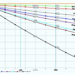
- Figure 4. Loss vs. Frequency of materials available for high speed
The state of technology
At the start of 21st century, providers of equipment for the Internet struggled to design large routers and switches containing backplanes and plug-in line cards that had long internal connections running at 3.125 Gb/s. The primary concern was how to manage loss in those long paths.
Fast forward to 2016 and the picture has changed radically. Manufacturers of the semiconductors used in route processors and switch ICs have managed to engineer them so they operate at speeds as high as 32 Gb/s with a very high tolerance for loss along the signal paths. The ICs of 2001 could tolerate as little as 10 dB of loss in the signal path at 3.125 Gb/s. The ICs of 2016 can tolerate as much as 38 dB of loss at 32 Gb/s.
These changes have exposed a number of microdefects in the signal path that were of little consequence in previous products running at lower data rates. These microdefects include:
1. The parasitic capacitance of the plated through holes required to mount the connectors can introduce substantial bandwidth degradation.
2. Crosstalk between transmit and receive signals can be severe because those signals that tolerate 38 dB of loss at the receivers are far more susceptible to interference from a signal leaving a transmitter at full amplitude.
3. The difference in travel time of the two sides of a differential pair (skew) induced by the irregularities in the weave of the glass cloth required to provide mechanical strength in the PCB can cause a signal path to fail.
4. Signal loss along the data paths is still an issue but, in most cases, can be handled with the materials currently available used to fabricate PCBs and backplanes. However, as the shift is made to 56 Gb/s and higher, loss in the data path comes back into the equation as a major issue.
Solving the first three problems has met with varied success.
The first problem (excess capacitance in the plated through holes) has been dealt with by using a technique called back-drilling to remove the excess capacitance of the connector plated through holes that extend below the layer in which the signal traces are routed. In thick backplanes this has resulted in very complex manufacturing procedures to ensure enough of the plated through hole copper has been removed to achieve proper performance while at the same avoiding drilling so deep that the connection is severed.
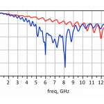
Figure 1 is a loss vs. frequency plot of two 8” (20 cm) traces. The red trace is routed near the bottom of the PCB so that the signal travels nearly the full length of the vias used to connect to the trace. The blue trace is routed near the top of the PCB so that the signal travels only part of the way along the vias leaving small parasitic capacitors attached to each end of the trace. Clearly, the bandwidth of the blue trace has been severely affected by these parasitic capacitors. Back drilling removes this unwanted parasitic with the risks noted earlier.
The second problem (excess crosstalk) has been dealt with by routing the signals farther and farther apart from each other so this problem is minimized. However, when receive signals can be only 2 or 3% the amplitude of transmit signals this becomes mechanically very difficult to accomplish when routing signals on the same layer in the vicinity of the connectors.
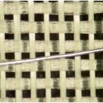
The third of these (skew or difference in travel time in the two sides of a differential pair), is a result of the uneven distribution of the glass in the woven cloth and the resin used to bind the composite together. This unevenness is due to the fact that the glass bundles used to weave the cloth are much larger than the width of the traces. Figure 2 is a photo of a common glass weave cloth (1080) with a 3.5 mil (89 micron) wire superimposed on it to show the difference in scale of traces and glass weaves. Notice that for part of the time the wire is on top of a glass bundle with a dielectric constant of about 6 and part of the time it is in between glass bundles in pure resin that has a dielectric constant of about 3. Signals will travel faster when they are in pure resin than when they are traveling over glass. This variation in velocity is what causes differences in travel time between the two sides of a differential pair. We have seen differences in travel time over 14 inch (35 cm) differential pairs on 1080 glass as high as 62 ps. That is 60% of a bit period at 10 Gb/s and two bit periods at 32 Gb/s.
Many techniques have been proposed to minimize the effect of skew. The two most common methods in use are:
• Routing the signals at an angle to the glass weave hoping that the irregularities are evened out between the two sides of the pair.
• Using a glass weave style that has the glass evenly spread out to minimize variation in the glass weave over which signals travel.
The first of these two methods has taken two forms. One is to route the signals in the PCB at an angle so that when the PCB is fabricated the traces run at an angle to the glass cloth weave. This has proved impractical in most products because the large number of connector and component pins impose an X-Y grid on routing.
Alternatively, the PCB or backplane is routed on an X-Y orientation and the artwork is placed at an angle on the fabrication panel resulting in the traces running at an angle to the glass weave. This method wastes substantial amounts of board material on the fabrication panels which are rectangles and thus increases overall board cost.
Neither of these methods are satisfactory for most products which must compete in a price-sensitive market.
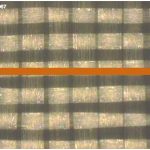
The second method employs a glass weave style that has the glass uniformly spread across the surface. Figure 3 is a photo of 1067 glass weave cloth with a 4 mil (102 micron) trace running across it. As can be seen, there are no resin filled voids in the example. Because of this, the difference in travel time of the two sides of the differential pair is minimized. In fact, we have been able to build quite large systems where the skew over 30 inches (76 cm) is less than 2 ps.
This sounds like the perfect answer to the skew problem. It would be if the methods by which the glass is spread were uniform between glass weavers. Unfortunately, this has proven not to be true. The driver for spreading the glass weave is the cell phone manufacturers. Their reason for spreading the glass is to make laser drilling of blind vias more uniform, not to preserve signal integrity. At present, there is no sure way to guarantee uniform spreading of the glass, so controlling skew by manipulating PCB laminates is problematic.
Dealing with signal-path loss
As mentioned at the start of this article, advances in semiconductor technology have resulted in transceivers that can tolerate as much as 38 dB of loss in the signal path at 32 Gb/s. This has made it possible to design systems with large backplanes with plug in modules. When the move to 56 Gb/s is made the materials that are available as laminates no longer have loss values that allow the design of the very large routers required in server farms and large IT centers. Figure 4 is the loss vs. frequency for a variety of materials that might be used to create next generation high performance Internet products.
Notice that the two curves labeled “cable” have far lower loss than any of the laminate systems used to manufacture current products. This loss is representative of what twinax cable can achieve. This solves the problem of how to achieve 56 Gb/s in large systems without the need to resort to optical interconnects.
More reliable & economical than PCB laminates
Since the signal integrity problem at high data rates in large systems is directly traced to microdefects in the PCBs and connectors used to manufacture very large, high performance systems, removing these signals from those PCBs and backplanes can solve the problem. This is not a new idea. If one looks back to several of the high performance computers designed by Cray Research and other companies in that market, all of the very high speed signals were moved from PCB to PCB over shielded twisted pairs or, in some cases, unshielded twisted pairs. This latter technique is how the Ethernet has been able to operate over long distances using ordinary phone wiring at data rates as high as 1 Gb/s.
The first advantage of the cable method is the opportunity for crosstalk between signals to be eliminated.
A second advantage the cable method has is the backplane can now be manufactured from standard PCB laminate material as its only task is to carry power to the modules plugged into it and to hold all of the connectors in a rigid structure.
What about the problem caused by those plated through holes that are necessary to hold the connector pins in place as well as the plated through holes required to connect component pins to traces in the daughter cards? What has been demonstrated by simulations as well as by laboratory measurement is that when a signal travels the length of the plated through hole or via, the parasitic capacitance of the hole is distributed along the length of the hole, rendering it virtually invisible.
This leaves the task of tackling skew. When the differential pairs are connected with shielded pairs, such as twinax, the two sides of the differential pair travel in a very uniform dielectric that is common to both sides of the pair. The result is that skew or difference in travel time between the two sides of a pair can be made virtually zero.
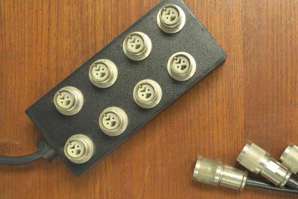
Figure 5 is an example of a design that uses this twinax method to implement a very complex high performance switch/router. Using this method, performance as high as 56 Gb/s can be achieved using ordinary PCB materials. This avoids the problem of designing very complex PCBs and then managing the supply chain process to insure that all of the complex manufacturing problems are kept under control.
Figure 6 shows the loss vs. frequency of several 2.6m – 3m differential paths. The measured paths include two daughter cards connected through twinax cable as shown in Figure 5. The insertion loss is near ideal up to about 25 GHz. This demonstrates that this assembly is potentially capable of 50 Gb/s.
A further advantage of implementing all of the high performance signals in twinax cable is that it is possible to make wiring changes at the backplane level by reconfiguring the twinax cables to implement a new function not available when the original backplane design is done. This helps eliminate the “fork lift” upgrades often required with hard wired backplanes.
Conclusion
Advances in semiconductor technology are making it possible to connect components in products such as switches and routers at rates as high as 56 Gb/s. As these higher speeds are achieved, micro-scale variations in the materials used to fabricate PCBs and backplanes can significantly degrade signals. Among the problems encountered are loss, skew, crosstalk, and degradation due to the parasitic capacitance of the plated-though holes required to mount the connectors to the backplanes and daughter cards.
By using twinax cables to make these connections instead of implementing them in PCBs and backplanes with traditional traces, skew, crosstalk, and degradation from the plated-though holes can be virtually eliminated. Due to the ultra-low loss of the twinax cables, path lengths can be longer, or the frequency of operation can extend much higher than is possible with the laminate systems currently available.
Authors Ritchey & Knack are with Speeding Edge, McMorrow with Samtec division Teraspeed Consulting.


