


EPFL researchers have printed nanometric-scale sensors capable of improving the performance of atomic force microscopes.
Tiny sensors made through nanoscale 3D printing may be the basis for the next generation of atomic force microscopes. These nanosensors can enhance the microscopes’ sensitivity and detection speed by miniaturizing their detection component up to 100 times. The sensors were used in a real-world application for the first time at EPFL, and the results are published in Nature Communications.
A tiny turntable that ‘listens’ to atoms
Atomic force microscopy is based on powerful technology that works a little like a miniature turntable. A tiny cantilever with a nanometric tip passes over a sample and traces its relief, atom by atom. The tip’s infinitesimal up-and-down movements are picked up by a sensor so that the sample’s topography can be determined.
One way to improve atomic force microscopes is to miniaturize the cantilever, as this will reduce inertia, increase sensitivity, and speed up detection. Researchers at EPFL’s Laboratory for Bio- and Nano-Instrumentation achieved this by equipping the cantilever with a 5-nanometer thick sensor made with a nanoscale 3D-printing technique. “Using our method, the cantilever can be 100 times smaller,” says Georg Fantner, the lab’s director.
Electrons that jump over obstacles
The nanometric tip’s up-and-down movements can be measured through the deformation of the sensor placed at the fixed end of the cantilever. But because the researchers were dealing with minute movements – smaller than an atom – they had to pull a trick out of their hat.
Together with Michael Huth’s lab at Goethe Universität at Frankfurt am Main, they developed a sensor made up of highly conductive platinum nanoparticles surrounded by an insulating carbon matrix. Under normal conditions, the carbon isolates the electrons. But at the nano-scale, a quantum effect comes into play: some electrons jump through the insulating material and travel from one nanoparticle to the next. “It’s sort of like if people walking on a path came up against a wall and only the courageous few managed to climb over it,” said Fantner.
When the shape of the sensor changes, the nanoparticles move further away from each other and the electrons jump between them less frequently. Changes in the current thus reveal the deformation of the sensor and the composition of the sample.
Tailor-made sensors
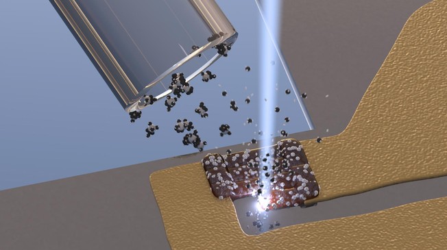
The researchers’ real feat was in finding a way to produce these sensors in nanoscale dimensions while carefully controlling their structure and, by extension, their properties. “In a vacuum, we distribute a precursor gas containing platinum and carbon atoms over a substrate. Then we apply an electron beam. The platinum atoms gather and form nanoparticles, and the carbon atoms naturally form a matrix around them,” said Maja Dukic, the article’s lead author. “By repeating this process, we can build sensors with any thickness and shape we want. We have proven that we could build these sensors and that they work on existing infrastructures. Our technique can now be used for broader applications, ranging from biosensors, ABS sensors for cars, to touch sensors on flexible membranes in prosthetics and artificial skin.”
—–
Source: Direct-write nanoscale printing of nanogranular tunnelling strain sensors for sub-micrometre cantilevers