A slowdown of the storage density scaling trend
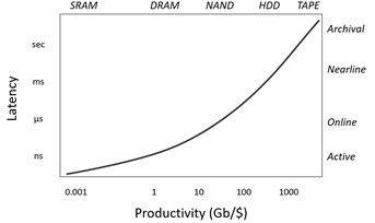
Today’s memory landscape comprises diverse types of memory, each of which plays its part in storing the data and feeding them back and forth to the computational part of the electronic system. In traditional computer hierarchies, fast and more expensive active memories (static random access memory (SRAM) and dynamic RAM (DRAM)) are distinguished from higher-latency and lower-cost storage solutions.
Storing large amounts of data is primarily accomplished by NAND-Flash, hard disk drive (HDD), and tape technologies. While tape storage remains limited to long-term archiving, HDD and NAND-Flash are used for online and nearline storage applications: they both need to be accessed more frequently than tapes, with access times ranging from microseconds to seconds. NAND-Flash offers the lowest latency and power consumption of these two storage types. This non-volatile memory is present in all major electronic end-use markets, such as smartphones, servers, PCs, tablets, and USB drives.
Figure 1 – Indicative overview of today’s main memory technologies and their application domains, illustrating the trade-off between latency and productivity (also presented at IMW 2022).
Researchers have been able to significantly improve the bit density of the various storage solutions throughout the years to keep up with the growing demand for bits per volume. However, for some years now, HDD technology has not been able to follow the historical productivity trendline. A similar time lag is expected for NAND-Flash technology. 3D-NAND-Flash is projected to reach storage densities of up to 70Gbit/mm2 by 2029, which is a slowing down of circa four years with respect to the historical density scaling roadmap.
Entering the post-NAND era
After NAND-Flash scaling has saturated, we expect different storage technologies to co-exist, each trading off size, energy consumption, latency, and cost. New concepts for storage are being investigated, not to replace the existing storage solutions but to complement them in the latency/productivity space. Think about DNA storage, targeting low-cost, ultrahigh-density but slow archival applications (such as preservation of (surveillance) video, medical and scientific data), or ferro-electric memory technology, projected to find its place in the lower-latency storage market segment. All these memories will be organized in different tiers and will jointly address the storage needs of the >100 zettabyte data era.
In this article, we propose two new liquid-based storage concepts – colloidal and electrolithic memory – with the potential for ultrahigh-density nearline storage applications. These storage solutions could, for example, make archived ‘inactive’ data such as email archives, image & sound files, or other large documents accessible to users within seconds. From 2030 on, they might find their place between HDD and tapes, at significantly higher bit per volume but slower than 3D-NAND-Flash.
Increasing the bit density requires new ways to address memory cells
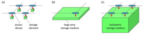
We believe there is a fundamental reason why it is challenging to scale further the bit densities of conventional solid-state memories (such as SRAM, DRAM, or 3D-NAND-Flash) cost-efficiently. In all these memories, the memory cells are organized in two- or three-dimensional arrays, at the cross-points of word- and bitlines. Each cell minimally consists of a storage element and an access device. The access device – usually a transistor or a diode – connects the storage element to at least two wires needed for selecting, reading, and writing the memory cell. The scaling challenge does not relate to the storage element itself (storage elements the size of a single molecule have already been demonstrated) but rather to the access device and its wiring. Cells are at least 2Fx2F (4F2) in size, with F the minimum feature size (for example, the wordline half-pitch) determined by the (expensive) lithography step used for patterning the wires. This configuration with one access device for each storage element makes it challenging to develop cost-efficient high-density solutions and store more than a few bits per cell (with 4-bit NAND-Flash cells currently being the maximum).
A different strategy is pursued by HDD and tape storage technologies. Here, a significantly smaller number of read/write access devices connect to a larger un-patterned area that serves as the storage medium. This leads to higher densities and lower cost per bit than NAND-Flash. But also to slower, bulkier and energy-consuming solutions – as the reading heads must be mechanically positioned over a large area.
Disruptive solutions couple a dense array of access devices to a volumetric storage medium
By reconciling the best of both worlds, new approaches can be found for making ultrahigh-density storage devices at an affordable cost per bit that operate faster than, for example, tapes. Why not make a dense array of access devices that connect to a volumetric storage medium? Inspired by advances in life sciences, this storage medium could be a liquid containing ions, molecules, or (nano-)particles, which can be manipulated and moved in larger volumes to an access device that is part of a dense array. This approach would enable multi-bit operation, with significantly fewer access devices, wires, and lithography steps needed per bit. The high-density potential of this new approach has attracted interest from industry, and several liquid-based concepts are being investigated worldwide.
Figure 2 – Three different types of addressing employed by memory technologies (also presented at IMW 2022).
Below, we propose two new liquid-based concepts with long-term potential for nearline storage, targeting (sub-)second access times. In this article, the focus is on their operating principle and first experimental results. More details were presented at IMW 2022 [1], and work on the electrolithic memory was recently published in IEEE Transactions on Electron Devices [2].
Colloidal memory: manipulating nanoparticles
A first liquid-based memory concept introduced by imec is referred to as the colloidal memory. It nicely shows how liquid (e.g., water) can be used as the volumetric storage medium and dissolved nanoparticles (the colloid) as carriers of the data symbols.
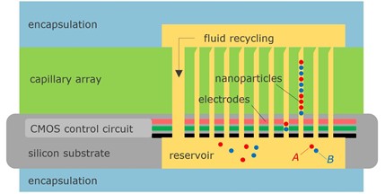
The idea is to use a colloid of (at least) two types of nanoparticles (A and B) contained in a reservoir. This reservoir is attached to an array of capillaries, into which the nanoparticles can be inserted. Provided that the nanoparticles are only slightly smaller than the diameter of the capillaries, the sequence in which the particles (the bits) are entered into the capillaries can be preserved. It is in this bit sequence that information can be encoded. The nanoparticles can be selectively induced (and sensed) by electrodes positioned at the entrance of each capillary. A CMOS peripheral circuit controls the array of electrodes.
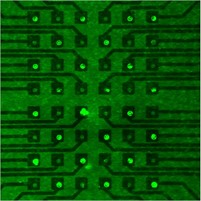
One of the main challenges relates to ‘writing’ the sequence of the nanoparticles, in other words, to attract and insert particles into the capillary selectively. Imec researchers are exploring both theoretically and experimentally the feasibility of using frequency-dependent dielectrophoresis as a write mechanism. Following this mechanism, an alternating electric field generated across the electrode exerts a force on the nanoparticle. Whether this force is attractive or repulsive depends, among other things, on the type of particle and the frequency of the evoked electric field. A selective writing process can be created by choosing two particles that respond differently to the applied frequency (attractive versus repulsive).
The colloidal memory technology is in an exploratory stage of research and development. The first set of experiments with µm-sized electrodes in different configurations (including interdigital and checkboard arranged arrays) marked the first milestone. Using the dielectrophoresis effect, they showed the feasibility of selectively extracting polystyrene nanoparticles from a mixed solution. But the required technology still needs significant development. Further investigations are ongoing to finetune the concept and provide the first proof of principle on a nanometer scale.
Figure 4 – Demonstration of the write process: (fluorescent) polystyrene nanoparticles are attracted by an alternating electric field generated by electrodes addressed in a checkboard arrangement.
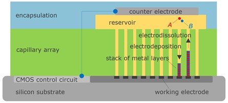
Electrolithic memory: exploiting electrochemistry
Like the colloidal memory, the electrolithic memory also uses a fluid reservoir and an array of capillaries. But in this case, metal ions are dissolved in the liquid, and the read and write operations are achieved by the more conventional electrodeposition and -dissolution techniques.
In more detail, the reservoir contains a fluid in which (at least) two metal ions (A and B) are dissolved. This reservoir connects to an array of capillaries (or wells). A working electrode (made of an inert metal such as ruthenium (Ru)) resides at the bottom of each capillary. The reservoir is also in contact with a single counter electrode. Together, the reservoir, the working electrode, and the common counter electrode form an electrochemical cell for each capillary. The dense array of working electrodes is connected to a CMOS integrated circuit for addressing each electrode individually.
By applying a certain potential at the working electrode within the capillary, thin layers of metal A can be deposited on the electrode. Metal B will behave similarly but deposits at a different onset potential – determined by its chemical nature. Information can now be encoded in the stack of alternating layers, suggestive of geolithical stone (lithos) strata – hence the name of the new memory.
We can now think of several ways to encode the information. In one possible encoding scheme, 1nm of metal A can be used to encode binary 0, while 2nm thick layers of A encodes a binary 1. A layer of metal B of fixed thickness (e.g., 0.5nm) can be used to delineate subsequent layers of A. In reality, assuming a higher onset potential of B compared to A, layers of metal B will be alloyed with some amount of A. Reading of the electrolithic memory can be realized by reversing the cell current and monitoring the dissolution potential.
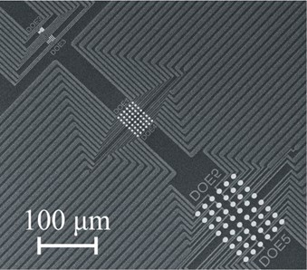
Figure 6 – Top view SEM showing microelectrode arrays with electrodes of different sizes in the mm- to µm-range: the first proof of concept (also presented at IMW 2022).
In a first proof-of-concept using mm- and µm-sized electrodes, the feasibility of using these techniques for reading and writing could be successfully demonstrated. For example, for a 4µm diameter electrode, the researchers demonstrated consecutive writing and reading of two layers of CoNi, alternated with three layers of Cu. The experiments also indicated shorter write/read times for µm-sized electrodes than larger ones.
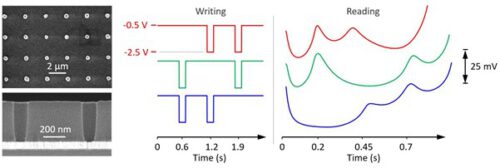
Nanometer-sized wells at tight pitches are eventually needed to achieve sufficiently high bit densities and response times. Therefore, the imec researchers fabricated the second generation of electrolithic memory cells, designed to write and read signals from an extensive array of parallelized nanowells (80 – 150nm diameter, 300nm deep). Preliminary results show that the read signals obtained after dissolving a Cu/CoNi five-layer stack correspond well to the writing (i.e., deposition) operation (see figure 7).
Figure 7 – (Left) Second generation of electrolithic memory cells with nanowells and common bottom electrode; (middle) schematic representation of writing the Cu/CoNi 5-layer stack, showing three different writing schemes; (right) read signals, clearly showing the position of the CoNi layer within the stacks. E.g., peaks that appear first in time correspond to the latest deposited CoNi layer.
Towards industrial adoption: improving density, response time, bandwidth, endurance, and retention
These new liquid-based memories are still in an exploratory research stage, with the electrolithic memory being the most advanced. Nevertheless, industry has already shown considerable interest in these concepts. At imec, we envisage their introduction in the memory roadmap from 2030 onwards, when the bit density scaling of 3D-NAND-Flash will start saturating.
With further scaling efforts, we anticipate that with these approaches, the bit storage density can be pushed towards the 1Tbit/mm2 range at a lower process cost per mm2 compared to 3D-NAND-Flash. For liquid memories, such an ultrahigh density can only be achieved if electrodes and capillaries are made on a pitch of 40nm. Also, researchers must be able to make capillaries with aspect ratios of about 400:1 and 165:1 for colloidal and electrolithic memory, respectively. This is similar to the aspect ratios of the memory holes needed for making future 3D-NAND-Flash products and is therefore considered a realistic target.
To become a viable storage solution for nearline applications, the technology must also have adequate response time, bandwidth (e.g. 20Gb/s), cycling endurance (103 write/read cycles), energy consumption (a few pJ to write a bit), and retention (over 10 years). These evaluations will be the subject of further research, building on imec’s 300mm liquid memory test platforms with both colloidal and electrolithic cells in different configurations.
Want to know more?
[1] ’Liquid memory and the future of data storage’ by M. Rosmeulen et al., invited paper at IMW 2022;
[2] ‘Electrolithic memory: a new device for ultra-high density data storage’ by S. Fransen et al., IEEE Transactions on Electron Devices, doi: 10.1109/TED.2022.3162176.
Further reading:
About the author
Maarten Rosmeulen
Maarten Rosmeulen received his M.Sc. degree in physics in 1993 and the M.Sc. degree in physics of micro-electronics and materials science in 1994, both from the KU Leuven, Belgium. In 2005, he received the Ph.D. degree in electrical engineering from the KU Leuven. Since then, he is with imec, Leuven, Belgium where he has been active as an R&D engineer in process integration, semiconductor device design and electrical device characterization for multiple internal and external projects. In 2009 he became project leader for the development of GaN-on-Silicon Light Emitting Diodes (LEDs). In 2014 he became team leader of the Pixel Design and Testing team and has been responsible for the development of CMOS Image Sensor (CIS) technologies. In 2019 he became program director of the Storage Memory program, the position he holds today.
This acquisition further establishes Quantum Machines as the quantum company with the broadest global footprint,…
Supporting planned growth in InP silicon photonics technology Resolving all prior IP disputes between the…
Norwest leads the round with strategic participation from Snowflake Ventures, as Jedify addresses the AI…
Round brings total funding to $15 million from U.S., European and Israeli investors to support…
Quantum Machines achieves 99.5% median two-qubit gate fidelity when operating Rigetti Computing’s Novera™ superconducting QPU…
Unframe, the managed AI delivery platform for global enterprises, today announced it has crossed $100…