Extended functionality, as well as decreased weight and heat dissipation, are at the core of electronic miniaturization technology. For decades, the microelectronic industry has been engaged in shrinking the transistor dimensions to enable this miniaturization for various applications (automotive, aerospace, medical industries, and others). Today, this miniaturization trend is no longer limited by the size of single transistors. Instead, the system size and reliability are dictated in many cases by the chip packaging and PCB sizes. Therefore, chip packaging technology becomes a key factor enabling smaller, lighter systems with increased functionality. To ensure system reliability and space reduction, the package should comply with several thermal, mechanical, and electrical requirements.
Semiconductor chips are the main building blocks of any digital signals processing device. Once assembled on top of a PCB, the gap between the semiconductor coefficient of thermal expansion (CTE for Silicon- 3 ppm/C˚) and the PCB (typical CTE of 15-20 ppm/C˚) becomes an obstacle. While the PCB dimensions expand during assembly and reflow processes, the chip remains almost intact. These changes result in mechanical stress, affecting the assembly process and hindering the system’s long-term reliability.
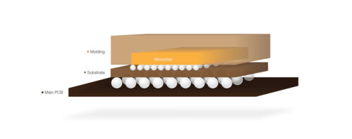
The most effective way to meet this challenge is by assembling the chips onto the PCB indirectly, using a substrate as an intermediate layer (see figure 1). The encapsulated chip-substrate stack, also known as a chip-scale package (CSP) is then soldered to the main PCB. To mitigate the CTE difference between the main PCB and chip, the substrate circuit should be made out of manufacturing-compatible material that has a CTE value of 5-7 ppm/C.
Another significant challenge in attaching a microchip to a PCB is the need for power dissipation. In high-end digital applications, transistor size comes at a price of increased power consumption. Other systems that use lower-end processors typically include analog devices such as receivers, transmitters, and power management components – all handle high currents. High power results in “hot spots” areas where chip temperature rises during operation. Failure to dissipate this heat causes the temperature to increase and reduces functionality and reliability risk. PCB manufacturing utilizes several solutions for heat dissipation- all rely on the thermal conductivity of copper coins used as heat sinks. However, these solutions are incompatible with microchip assembly, due to the high level of Cu CTE (17 ppm/C). An effective solution, combining high thermal conductivity (typical values above 200 W/mK) with low CTE (5-7 ppm/C) can be realized by creating a laminate comprised of copper and refractory metals. In such laminates, copper is responsible for thermal conductivity while the refractory metal ensures low CTE. The actual thermal conductivity / CTE is determined by the relative thickness of each metal.
The ability to design and manufacture advanced substrates – including low-CTE heat sinks clears the way for advanced systems, where more than one chip can be mounted onto the same substrate. Forming this System in Package (SIP) allows several types of microchips, from several vendors and produced with different semiconductor technologies, to be assembled on one substrate. The substrate can also include analog devices (e.g. resistors) and miniature PCB line/space enabling chip connectivity with a shorter path thus using a smaller PCB footprint. Furthermore, the substrate enables to stack microchips resulting in a 3D package that is in itself a full system.
SiP can be used in any application that benefits from miniaturization- for example, any transmitter/receiver system- including radars for autonomous vehicles, military radar systems, cellphones, etc. The main component in such systems is a transmitter/receiver chip, usually GaAs-based. The receiver is a high-power chip, requiring heat dissipation. In addition, the system requires a data processing component and antenna switches, typically realized by Si-based chips. Assembling and encapsulating each of these chips separately might result in large PCB footprint consumption. Furthermore, the electrical connection between chips relies on long interconnects – limiting the system speed and wasting power. Packing all these chips on one substrate means that the whole system area can be reduced by a factor of 4-10. Many analog devices that are needed as part of the circuit can also be mounted on the same SiP – resulting in a smaller, faster system.
Another good example is navigation systems, which include micro-electromechanical systems (MEMS) chips as well as data processing and analysis chips. Such systems are becoming widespread and are critical for autonomous vehicles, self-propelled drones, cellphones, etc.
Designers normally engage with several vendors for the development of a new system based on SiP. One for SiP circuit design, another for manufacturing, a third vendor for chip assembly and encapsulation, and one or two additional vendors for PCB manufacturing and system assembly. The need to comply with so many manufacturers’ design rules, requires compromise, limits the system performance, and creates a significant delay in time to market.
PCB Technologies sets new standards of holistic engineering, saving our customers the time and energy required for coordinating between various suppliers. Our All-in-One approach enables combining various materials while tailoring the required properties for the customer’s PCB needs. We offer our customers the ability to design and manufacture substrates for microchip assembly, chip assembly, and encapsulation to create a system in package. A true one-stop-shop for any design or project.
Abstract – The Gyro klystrons are vacuum electronic devices which can produce high power in…
As hyperscalers race to build ever larger AI infrastructure, processors, networking and cooling often dominate…
More than 150 exhibiting companies representing thousands of leading technology manufacturers from Israel and around…
Akamai Technologies, Inc. (NASDAQ: AKAM) announces the company has completed its acquisition of secure enterprise…
Partnership brings UVeye’s state-of-the-art inspection technology to the middle mile, enhancing safety, consistency, and efficiency…
The collaboration brings NVIDIA Isaac GR00T 1.7 and Isaac Teleop to the LeRobot platform, giving…