The company’s $26 billion in 2017 outlays expected to be more than Intel and TSMC combined.
IC Insights has revised its outlook for semiconductor industry capital spending and will present its new findings in the November Update to The McClean Report 2017, which will be released at the end of this month. IC Insights’ latest forecast now shows semiconductor industry capital spending climbing 35% this year to $90.8 billion.
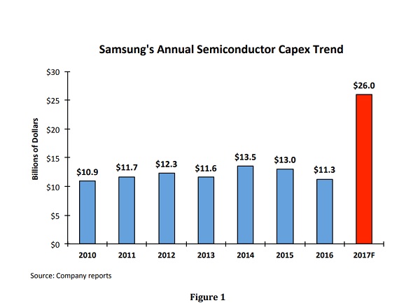
After spending $11.3 billion in semiconductor capex last year, Samsung announced that its 2017 outlays for the semiconductor group are expected to more than double to $26 billion. Bill McClean, president of IC Insights stated, “In my 37 years of tracking the semiconductor industry, I have never seen such an aggressive ramp of semiconductor capital expenditures. The sheer magnitude of Samsung’s spending this year is unprecedented in the history of the semiconductor industry!”
Figure 1 shows Samsung’s capital spending outlays for its semiconductor group since 2010, the first year the company spent more than $10 billion in capex for the semiconductor segment. After spending $11.3 billion in 2016, the jump in capex expected for this year is simply amazing.
To illustrate how forceful its spending plans are, IC Insights anticipates that Samsung’s semiconductor capex of $8.6 billion in 4Q17 will represent 33% of the $26.2 billion in total semiconductor industry capital spending for this quarter. Meanwhile, the company is expected to account for about 16% of worldwide semiconductor sales in 4Q17.
IC Insights estimates that Samsung’s $26 billion in semiconductor outlays this year will be segmented as follows:
3D NAND flash: $14 billion (including an enormous ramp in capacity at its Pyeongtaek fab)
DRAM: $7 billion (for process migration and additional capacity to make up for capacity loss due to migration)
Foundry/Other: $5 billion (for ramping up 10nm process capacity)
IC Insights believes that Samsung’s massive spending outlays this year will have repercussions far into the future. One of the effects likely to occur is a period of overcapacity in the 3D NAND flash market. This overcapacity situation will not only be due to Samsung’s huge spending for 3D NAND flash, but also to its competitors in this market segment (e.g., SK Hynix, Micron, Toshiba, Intel, etc.) responding to the company’s spending surge. At some point, Samsung’s competitors will need to ramp up their capacity or loose market share.
Samsung’s current spending spree is also expected to just about kill any hopes that Chinese companies may have of becoming significant players in the 3D NAND flash or DRAM markets. As our clients have been aware of for some time, IC Insights has been extremely skeptical about the ability of new Chinese startups to compete with Samsung, SK Hynix, and Micron with regards to 3D NAND and DRAM technology. This year’s level of spending by Samsung just about guarantees that without some type of joint venture with a large existing memory suppler, new Chinese memory startups stand little chance of competing on the same level as today’s leading suppliers.
Dual-side cooling (DSC) shrinks package footprint by 57% compared with TOLT, packing more power into…
Supporting manufacturers with reliable defect identification and scalable quality control across production lines Leica Microsystems,…
The Magnum E2 system supports emerging DRAM and NAND interfaces while using common hardware and…
The first unmanned ground systems left the production line only 12 weeks after the two…
The available-now engineering assistant connects language models to AMD development tools, documentation and reusable FPGA…
The 0.6 × 0.3 mm capacitors occupy 64% less mounting area than Murata’s previous smallest…