
How to use a low-cost microcontroller as a driver for a single-winding, single-phase brushless DC motor
In a low-power motor application, where cost is more important than complexity and torque requirements are reduced, a single-phase brushless DC (BLDC) motor is a good alternative to a three-phase motor.
This type of motor is low cost because of its simple construction, which is easier to fabricate. Also, it only requires a single-position sensor and a few driver switches to control and energise the motor winding. Therefore, the trade-off between motor and control electronics can work out favourably.
To maintain the cost effectiveness, a low-cost motor driver is needed. The driver circuit described here can exploit two feedback loops. The first, the inner loop, is responsible for commutation control, while the second, the outer loop, handles speed control. The speed of the motor is referenced to an external analogue voltage and fault detection can be sensed during over-current and over-temperature conditions.
Fig. 1 shows the single-phase driver based on Microchip’s PIC16F1613 8bit microcontroller, chosen because of its low pin count and on-chip peripherals that can control the driver switches, measure the motor speed, predict the rotor position and implement fault detection. This application uses the following peripherals: complementary waveform generator (CWG); signal measurement timer (SMT); analogue-to-digital converter (ADC); digital-to-analogue converter (DAC); capture compare PWM (CCP); fixed voltage reference (FVR): timer; comparator; and temperature indicator. These peripherals are internally connected by firmware, which reduces the number of external pins required.
The full-bridge circuit, which energises the motor winding, is controlled by the CWG output. A Hall sensor is used to determine the rotor position. Current that passes through the motor winding is translated into a voltage through the sense resistor Rshunt for over-current protection. The speed can be referenced in an external analogue input. Fig. 2 shows the control diagram of the motor driver; for this application, the rated motor voltage is 5V and rated speed 2400rev/min. The motor driver supply voltage is 9V.
The speed reference can be any analogue input. The microcontroller’s ADC module has 10bit resolution and up to eight channels, making its suitable for different kinds of analogue input. This is being used to derive the speed reference and the initial PWM duty cycle, used to initialise the speed of the motor based on the source of the speed reference.
The initial duty cycle can be increased or reduced by the result of the proportional-integral (PI) controller and the new duty cycle value loaded in the CCP, the PWM output of which is used as the initial source of the CWG to control the modulation of the lower side switches of the full-bridge driver and, hence, the speed of the motor.
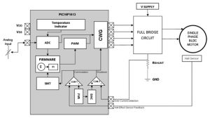
Fig. 1: Block diagram of single-phase BLDC driver
Inner loop
The inner feedback loop is responsible for commutation control. The CWG output, which controls the excitation of the stator winding, depends on the state of the Hall sensor output, which is compared with an FVR by the comparator. The comparator hysteresis is enabled to disregard the noise in the sensor output.
The output of the comparator toggles between forward and reverse full bridge mode to produce clockwise or anti-clockwise rotation. The CWG output is fed to the switches’ input of the full bridge circuit.
To produce one electrical cycle, a forward-reverse combination must be executed. One mechanical revolution of the motor requires two electrical cycles, therefore two forward-reverse combinations must be executed to complete a single clockwise rotation of the motor.
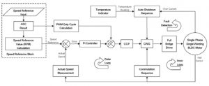
Fig. 2: Control diagram of motor driver
Full-bridge circuit
The full-bridge circuit in Fig. 3 is primarily composed of two p-channel MOSFETs as high-side switches and two n-channel MOSFETs as low-side switches. The main advantage of the p-channel transistor is the simplicity of the gate-driving technique in the high-side switch position, thus reducing the cost of the high-side gate-driving circuit.
Even though the high- and low-side switches can be switched on at the same time – cross conduction – this kind of switching should be avoided otherwise it will create a current shoot-through that might damage the driver’s components. To avoid this, a dead-band delay can be implemented using the CWG’s counter registers. This provides non-overlapping output signals that stop the high- and low-side conducting at the same time.
Ideally, the n- and p-channel MOSFETs should have the same on resistance (RDSon) and total gate charge QG to obtain the optimal switching performance. Therefore, while it would be good to choose a complementary pair of MOSFETs to match these parameters, in reality this is impossible due to their different construction; the chip size of the p-channel device must be two to three times that of the n-channel to match the RDSon performance. But the larger the chip size, the larger the effect of QG. Thus, when selecting the MOSFETs, it is important to decide whether RDSon or QG will have the biggest impact on switching performance and choose accordingly.
Fault detection
Exceeding the motor’s maximum allowable torque loading can cause the motor to stall and the winding to take the full current. Thus, to protect the motor, fault detection for over current and stalling must be implemented.
To implement over-current detection, Rshunt is added to the drive circuitry, which gives a voltage corresponding to the current flowing in the motor winding. The voltage drop across the resistor varies linearly with respect to the motor current. This voltage is fed to the inverting input of the comparator and compared with a reference voltage based on the product of Rshunt resistance and the maximum allowable stall current of the motor.
The reference voltage can be provided by the FVR and can be narrowed down further by the DAC. This allows a very small reference voltage to be used, which lets the resistance be kept low thus reducing power dissipation from Rshunt. If the Rshunt voltage exceeds the reference, the comparator output triggers the auto-shutdown feature of the CWG, the output of which will remain inactive as long as the fault exists.
Over temperature can be detected using the device’s on-chip temperature indicator, which can measure temperatures between -40 and +85˚C. The indicator’s internal circuit produces a variable voltage relative to temperature and this voltage is converted to digital by the ADC. For a more accurate temperature indicator, a single-point calibration can be implemented.
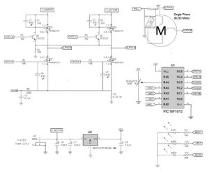
Fig. 3: Single-phase BLDC motor driver schematic diagram
Outer loop
The outer loop shown in Fig. 2 controls the motor’s speed under varying conditions such as changes in load demand, disturbances and temperature drift. The speed is measured by the SMT, which is a 24bit counter-timer with clock and gating logic that can be configured for measuring various digital signal parameters such as pulse width, frequency, duty cycle and the time difference between edges on two input signals.
Measuring the motor’s output frequency can be done through the SMT’s period and duty cycle acquisition mode. In this mode, either the duty cycle or period of the SMT signal can be acquired relative to the SMT clock. The SMT counts the number of SMT clocks present in a single period of motor rotation and stores the result in the captured period register. Using this register allows the actual frequency of the motor to be obtained.
When the speed reference is compared with the actual speed, it will yield a positive or negative error depending on whether the actual speed is higher or lower than the set reference. This error is fed to the PI controller, which is a firmware algorithm that calculates a value that compensates for the variation in speed. This compensating value will add to or subtract from the initial PWM duty cycle to produce a new value.
Conclusion
In cost-sensitive motor control applications, an efficient and flexible microcontroller can have significant impact. Device efficiency can be measured against the level of integrated peripherals to optimise the control task along with the number of pins and memory and the size of the package. Additionally, ease of use and time to market are important especially if variants of the design are required.
This article has shown how a low-cost microcontroller can meet these requirements and let the driver set the desired speed reference, predict the rotor position, implement a control algorithm, measure the actual speed of the motor and impose fault detection.This type of motor is low cost because of its simple construction, which is easier to fabricate. Also, it only requires a single-position sensor and a few driver switches to control and energise the motor winding. Therefore, the trade-off between motor and control electronics can work out favourably.
To maintain the cost effectiveness, a low-cost motor driver is needed. The driver circuit described here can exploit two feedback loops. The first, the inner loop, is responsible for commutation control, while the second, the outer loop, handles speed control. The speed of the motor is referenced to an external analogue voltage and fault detection can be sensed during over-current and over-temperature conditions.
Fig. 1 shows the single-phase driver based on Microchip’s PIC16F1613 8bit microcontroller, chosen because of its low pin count and on-chip peripherals that can control the driver switches, measure the motor speed, predict the rotor position and implement fault detection. This application uses the following peripherals: complementary waveform generator (CWG); signal measurement timer (SMT); analogue-to-digital converter (ADC); digital-to-analogue converter (DAC); capture compare PWM (CCP); fixed voltage reference (FVR): timer; comparator; and temperature indicator. These peripherals are internally connected by firmware, which reduces the number of external pins required.
The full-bridge circuit, which energises the motor winding, is controlled by the CWG output. A Hall sensor is used to determine the rotor position. Current that passes through the motor winding is translated into a voltage through the sense resistor Rshunt for over-current protection. The speed can be referenced in an external analogue input. Fig. 2 shows the control diagram of the motor driver; for this application, the rated motor voltage is 5V and rated speed 2400rev/min. The motor driver supply voltage is 9V.
The speed reference can be any analogue input. The microcontroller’s ADC module has 10bit resolution and up to eight channels, making its suitable for different kinds of analogue input. This is being used to derive the speed reference and the initial PWM duty cycle, used to initialise the speed of the motor based on the source of the speed reference.
The initial duty cycle can be increased or reduced by the result of the proportional-integral (PI) controller and the new duty cycle value loaded in the CCP, the PWM output of which is used as the initial source of the CWG to control the modulation of the lower side switches of the full-bridge driver and, hence, the speed of the motor.
Inner loop
The inner feedback loop is responsible for commutation control. The CWG output, which controls the excitation of the stator winding, depends on the state of the Hall sensor output, which is compared with an FVR by the comparator. The comparator hysteresis is enabled to disregard the noise in the sensor output.
The output of the comparator toggles between forward and reverse full bridge mode to produce clockwise or anti-clockwise rotation. The CWG output is fed to the switches’ input of the full bridge circuit.
To produce one electrical cycle, a forward-reverse combination must be executed. One mechanical revolution of the motor requires two electrical cycles, therefore two forward-reverse combinations must be executed to complete a single clockwise rotation of the motor.
Full-bridge circuit
The full-bridge circuit in Fig. 3 is primarily composed of two p-channel MOSFETs as high-side switches and two n-channel MOSFETs as low-side switches. The main advantage of the p-channel transistor is the simplicity of the gate-driving technique in the high-side switch position, thus reducing the cost of the high-side gate-driving circuit.
Even though the high- and low-side switches can be switched on at the same time – cross conduction – this kind of switching should be avoided otherwise it will create a current shoot-through that might damage the driver’s components. To avoid this, a dead-band delay can be implemented using the CWG’s counter registers. This provides non-overlapping output signals that stop the high- and low-side conducting at the same time.
Ideally, the n- and p-channel MOSFETs should have the same on resistance (RDSon) and total gate charge QG to obtain the optimal switching performance. Therefore, while it would be good to choose a complementary pair of MOSFETs to match these parameters, in reality this is impossible due to their different construction; the chip size of the p-channel device must be two to three times that of the n-channel to match the RDSon performance. But the larger the chip size, the larger the effect of QG. Thus, when selecting the MOSFETs, it is important to decide whether RDSon or QG will have the biggest impact on switching performance and choose accordingly.
Fault detection
Exceeding the motor’s maximum allowable torque loading can cause the motor to stall and the winding to take the full current. Thus, to protect the motor, fault detection for over current and stalling must be implemented.
To implement over-current detection, Rshunt is added to the drive circuitry, which gives a voltage corresponding to the current flowing in the motor winding. The voltage drop across the resistor varies linearly with respect to the motor current. This voltage is fed to the inverting input of the comparator and compared with a reference voltage based on the product of Rshunt resistance and the maximum allowable stall current of the motor.
The reference voltage can be provided by the FVR and can be narrowed down further by the DAC. This allows a very small reference voltage to be used, which lets the resistance be kept low thus reducing power dissipation from Rshunt. If the Rshunt voltage exceeds the reference, the comparator output triggers the auto-shutdown feature of the CWG, the output of which will remain inactive as long as the fault exists.
Over temperature can be detected using the device’s on-chip temperature indicator, which can measure temperatures between -40 and +85˚C. The indicator’s internal circuit produces a variable voltage relative to temperature and this voltage is converted to digital by the ADC. For a more accurate temperature indicator, a single-point calibration can be implemented.
Outer loop
The outer loop shown in Fig. 2 controls the motor’s speed under varying conditions such as changes in load demand, disturbances and temperature drift. The speed is measured by the SMT, which is a 24bit counter-timer with clock and gating logic that can be configured for measuring various digital signal parameters such as pulse width, frequency, duty cycle and the time difference between edges on two input signals.
Measuring the motor’s output frequency can be done through the SMT’s period and duty cycle acquisition mode. In this mode, either the duty cycle or period of the SMT signal can be acquired relative to the SMT clock. The SMT counts the number of SMT clocks present in a single period of motor rotation and stores the result in the captured period register. Using this register allows the actual frequency of the motor to be obtained.
When the speed reference is compared with the actual speed, it will yield a positive or negative error depending on whether the actual speed is higher or lower than the set reference. This error is fed to the PI controller, which is a firmware algorithm that calculates a value that compensates for the variation in speed. This compensating value will add to or subtract from the initial PWM duty cycle to produce a new value.
Conclusion
In cost-sensitive motor control applications, an efficient and flexible microcontroller can have significant impact. Device efficiency can be measured against the level of integrated peripherals to optimise the control task along with the number of pins and memory and the size of the package. Additionally, ease of use and time to market are important especially if variants of the design are required.
This article has shown how a low-cost microcontroller can meet these requirements and let the driver set the desired speed reference, predict the rotor position, implement a control algorithm, measure the actual speed of the motor and impose fault detection.